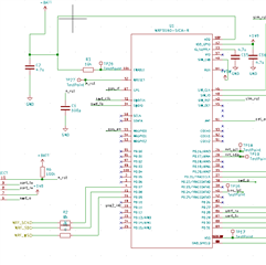
HI ,
On my costume board works fine when VDD connected to ~3.6v.
it starts to behave differently when voltage is ~4.1v. (Flashing fails / SW not loading ).
my VDD_GPIO is 1.8v.
Thanks,
Moshe
HI ,
On my costume board works fine when VDD connected to ~3.6v.
it starts to behave differently when voltage is ~4.1v. (Flashing fails / SW not loading ).
my VDD_GPIO is 1.8v.
Thanks,
Moshe
You don't say what processor you are using. That said, I'll guess the nRF52840 as a starting point. According to the OPS doc I have (may be out of date), that part is only rated up to VDD of 3.9V.
My apologies. I missed your tag. Wrong part.
Hi, are you using an onboard regulator or are you supplying the nRF91 directly? Is this the same board as you sent to us earlier for review? If so, I can try it out here and see what happens.
HI,
I'm not using an onboard regulator for the VDD (only for VDD_GPIO I use one).
it is not the same circuit as before.
please see the relevant circuit attached.
I got the full layout in a private ticket (251170). Copying my comment in that ticket for reference:
I think the problem is that you are using +BATT as the reference voltage on the debugger. The debugger sets the SWD lines to the same voltage as the vtref voltage, but on the nRF91 the SWD interface is connected to the VDD_GPIO domain (1.8V), so then you will be powering the VDD_GPIO domain through the SWD lines at 4.1V. Which will in the end destroy the chip.
Further you should remove the pullup on the reset pin (R6). The reset pin is internally connected to a 2.2V domain with it's own internal pullup, so by pulling it further up to VDD, you will get leakage current. It can be left unconnected when not in use.