This post is older than 2 years and might not be relevant anymore
More Info: Consider searching for newer posts

High voltage on open drain IO

Hi,

Can we give a voltage more than VDD+0.3V on an open drain high impedance configured IO pin? By open drain, I mean:

nrf_gpio_cfg(pin_num, NRF_GPIO_PIN_DIR_OUTPUT,
NRF_GPIO_PIN_INPUT_DISCONNECT,
NRF_GPIO_PIN_NOPULL,
GPIO_PIN_CNF_DRIVE_S0D1,
NRF_GPIO_PIN_NOSENSE );

Since its an open configuration, can it still damage the controller?

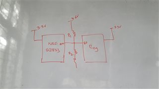
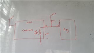
Due to a design error, we are getting 3.6V on an IO pin whereas the NRF VDD is at 2.5V.

We will fix this design error for future productions but for the current produced boards (which is quite a lot), I am wondering if the above workaround can be done.

Or is there any other pin configuration which can mitigate this damage?

Thank you,

Chethan

  • Hi Chethan,

    A voltage higher than VDD+0.3V coming from external chip will pass through an internal ESD protection diode and can damage the nRF chip if the signal is strong enough, despite of pin configuration. If there's only 3.6V coming from pull-up resistor, the bus will be clamped by nRF chip at 2.6-2.8V level - the damage is unlikely but other weird things can happen, nobody can guarantee a stable behavior in this case.

    See also this answer.

  • Correct. The ESD diodes will start to conduct of the GPIO voltage is VDD+0.3 V. If you have a series resistor, the current will be limited and the voltage is clamped to VDD+0.3 V on  the pin. Depending on the size of the resistor, this is fine. But of you pull the voltage higher than spec, you will start to lift the whole VDD net as well, and the current through the ESD diode will become to high and may damage the structure in the GPIO. 

  • Ok. Thanks for the clarification Dmitry and ketiljo.

    To give you more idea on the issue, here is our configuration:

    We operate on a 3.6V battery, which goes to a resistor divider. The output of resistor divider is about 2/3rd of the battery voltage.

    The output of voltage divider is fed to the enable pin of regulator and the adc pin (AIN0) of NRF52833. The output of regulator is configured to be for 3.3V.

    Ideally, the voltage divider should give us 2.4V with 3.6V battery. This works fine without NRF52833 connected.

    But with NRF52833 in picture, the voltage gets held up at 0.3V-0.5V.

    What could be the reason for this?

    Is the state of IO pin during startup causing the voltage to be clamped?

    We were thinking of bypassing this issue by shorting R1. But with the above behaviour, there might be more serious issues which can effect long term operation.

    Thank you,

    Chethan

  • But with NRF52833 in picture, the voltage gets held up at 0.3V-0.5V.

    That would be correct with NRF chips VDD at 0 Volt (LDO off).

    You will need a more complex startup curcuit here.

  • So the ESD diode clamps the voltage? Something like this:

    Can you please elaborate on the complex start up?

    The circuit gets started up with strong pull up or a diode on R1. Would this damage the IO pin or the controller?

    Thank you,

    Chethan

Related