This post is older than 2 years and might not be relevant anymore
More Info: Consider searching for newer posts

nRF52810 Design check

Hello,

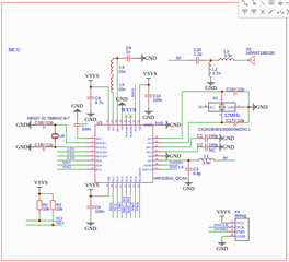
I am trying to develop BLE custom board. It's my first time dealing with Nordic MCUs and RF. I want to understand if I am doing it all correct. Here is a piece of my schematic:
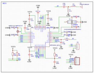
To provide RF front-end I choosed to use 2450AT18B100 chip antenna. I have a few questions:

1) Is my schematic correct?

2)Should I use impedance match IC (2450FM07A0029) instead of L1-C3 matching? What are the benefits of using this chip?

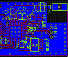
3) Is my PCB design correct (see pictures below), especially RF part?

4) Will my board work with default values (L1,C3,C20,L2,L3)? How should I tune this configuration to reach maximum range?

5) Is it ok to provide such reset circuit? Can I ommit it? If I can, are there any other options to reset the MCU?
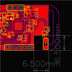
TOP PCB
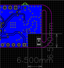
BOTTOM PCB

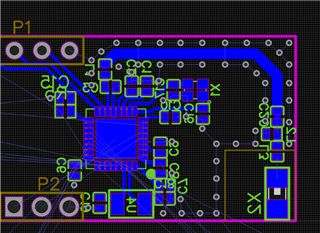
6) Also, will it be a better approach to turn MCU 90 degree counter-clockwise (like in picture below)? Which one is better for radio?

7) Can I move some parts like decouple capacitors and XTALS to the other side of the board?

8) Is it okay to use all R and C in 0402 package?
Thank you very much!

  • 1) Is my schematic correct?

    Yes, the schematic looks correct. 


    2)Should I use impedance match IC (2450FM07A0029) instead of L1-C3 matching? What are the benefits of using this chip?

     Only if you need the smaller size, else two components are more flexible. 


    3) Is my PCB design correct (see pictures below), especially RF part?

     Two things you need to fix:

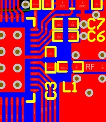
    1. C3 should be grounded only to the VSS_PA pin, like this: 

    2. Make a straight track to the antenna,. 

    Else it looks just fine. 


    5) Is it ok to provide such reset circuit? Can I ommit it? If I can, are there any other options to reset the MCU?

     You can remove R5 and C15 if you like as there are on-chip reset circuitry. 


    6) Also, will it be a better approach to turn MCU 90 degree counter-clockwise (like in picture below)? Which one is better for radio?

    Shorter track to the antenna is always better, less insertion loss.


    7) Can I move some parts like decouple capacitors and XTALS to the other side of the board?

     Yes, but keep the tracks short to the capacitors. 


    8) Is it okay to use all R and C in 0402 package?

     Yes, no problem.

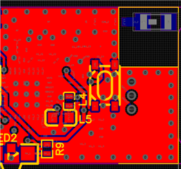
  • Thank you very much for your response! I've made the suggested changes. Also I've changed a little my schematic (removed reset circuit, added DC-DC components) Here I moved L4 and L5 to the other side of the board. Please take a short glance on my new design and say if it is acceptable.

    And a quick question: will XTAL in this design affect the radio? Isn't it too close to the antenna?

Related