
Hi,
I am using an nRF52 based chipset and programming the device with the hex file.This is being performed using the nRFConnect v.3.4.1 Programmer. The erase and write option is selected and this happens successfully without any issues. The memory gets read back and then the data in the application region is depicted in the slightly unique way to the way it was depicted from the hex file.
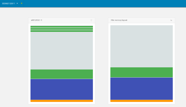
I again performed the same exercise/task using the nRF52 Dk Evaluation/Development board.Wherein , I programmed the device with the pre-generated hex file. But then again the memory organization seems to be slightly different and non-uniform .
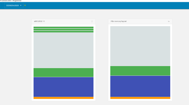
Is this a memory leak issue and will this create issues? I have seen the device functioning as intended. But the depiction is certainly worrying and hence need some clarity on this.
Note:- The hex files used over here have both the Softdevice - s132 and the application combined .
With Regards,
Samarth.
Cork.
