
Hi,
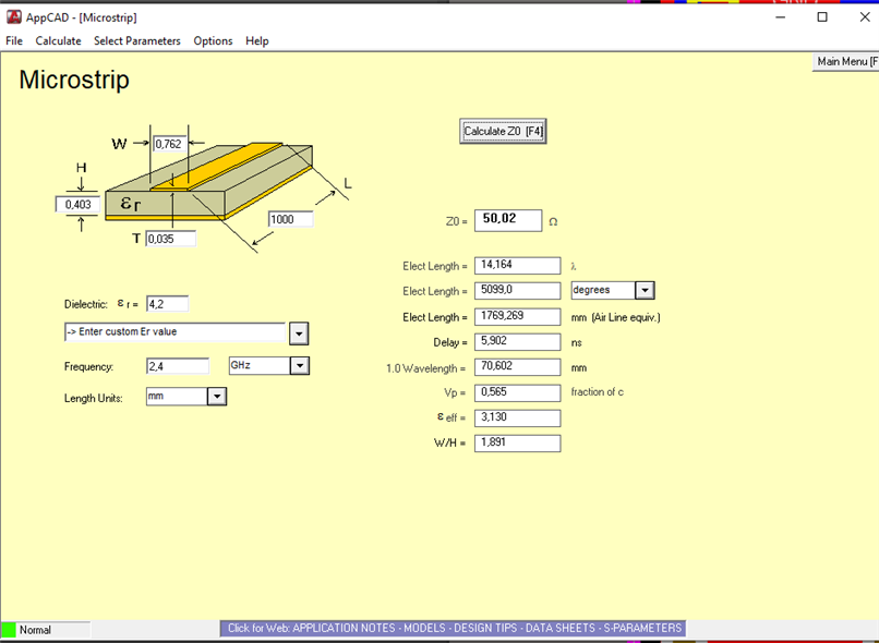
1 - I don't understand why on the PCB layout example the track that is connected the L2 inductor is 762µm thick while the thickness of the pcb is 0.8mm?
2 - To have an impedance of 50 ohms with this track width, isn't it necessary to have a PCB with a lower thickness (0.4mm)?
3 - What are the functions of components L1, L2 and C3? Is it just a low-pass filter?
4 - Can the L1, L2 and C3 components be replaced by this reference 2450FM07A0035 from Johanson technology?
Thank you in advance for your help.
Best regards
