Query on reference designs and layouts
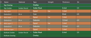
1. "nRF52833-QDAA Reference Layout 1_0 PCB" stack-up seems to need improvement (please check the Core thickness between Layer1 and Layer2. Whereas "nRF52833-QIAA Reference Layout 1_0" looks reasonable. Since we are using nRF52820-QDAA package, pls advise a reasonable reference layout. (reference Nordic website and NRF528xx reference design)
2. Seems L3 and L4 need to be swapped (L4 to be connected to U1-Pin 39 and L3 to the filter capacitors. (Reference nRF52820 datasheet, " Figure 149: Circuit configuration no. 2 schematics for QDAA QFN40 ")
Please correct me if my understanding is wrong and convince me with a suitable explanation.
General query
1. Is there any Nordic (or any third party) DVK with nRF52820 MCU?
Thanks