This post is older than 2 years and might not be relevant anymore
More Info: Consider searching for newer posts

Need some help with confusion about flash locations and size (nrf52832 + s132 6.1.1 softdevice)

Hi all,

Currently I am working on my first project with the nrf52832. All is going quite well, but I would really like some help with my flash layout, basically I got some confusion about the following:

Based on this post I figured my flash start position is at 0x26000 which is 155.648 in decimal. Now the nrf52832 which I am using has 256kb of flash memory, does this mean I only have (256 - 155 =) 101kb left for the firmware? My firmware is already bigger than that:

$ du -sh _build/nrfapp.bin
168K	_build/nrfapp.bin

I can flash it without problems and it works fine though. Am I working with wrong numbers?
This is how I would like the flash layout to look:

Content Start Address Size (bytes)
Firmware 0x26000 175000
AppData 0x50B98 4096

Could someone help me clear my confusion?

Thanks a lot!

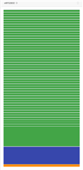
UPDATE: After writing this post I suddenly found a post where people recommended looking at the nRFConnect programmer. I figured my chip actually has 512kb of flash! I would still like to know if my approach is correct. Also, why does it look like this?:

Parents
  • Hi,

    Your calculations are correct. And using nRF Connect programmer for visualizing the memory layout quickly is a good idea.

    nRF Connect Programmer does not really know what is in the flash, so it makes assumptions. All the green sections are seen as application or application data, and the reason they are not consecutive is that there is chunks of erased flash in between for some reason. Perhaps you initialize a lot of FDS pages, or something else? What does your hex file(s) look like if you add them to the programmer app and look at them on the right-side panel? Do you still see all these chunks? If not, then this is because your firmware writes to that flash regions, or because of some "leftovers" from before if you have not done a full chip erase.

Reply
  • Hi,

    Your calculations are correct. And using nRF Connect programmer for visualizing the memory layout quickly is a good idea.

    nRF Connect Programmer does not really know what is in the flash, so it makes assumptions. All the green sections are seen as application or application data, and the reason they are not consecutive is that there is chunks of erased flash in between for some reason. Perhaps you initialize a lot of FDS pages, or something else? What does your hex file(s) look like if you add them to the programmer app and look at them on the right-side panel? Do you still see all these chunks? If not, then this is because your firmware writes to that flash regions, or because of some "leftovers" from before if you have not done a full chip erase.

Children
Related