Hello,
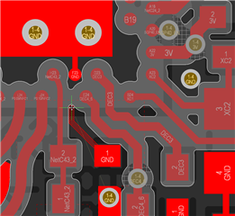
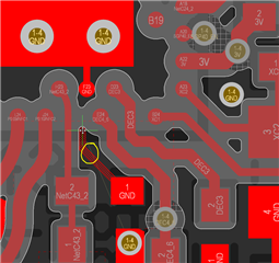
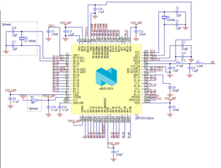
We are developing PBC with nRF52840 and we have problem regarding PCB layout. Because our PCB maker has minimal spacing between pad and track 0.2mm we can't make RF part of the layout like in the recommended nordic layout design. Is there any other way to route GND track to pin F23 within out PCB maker rules?