This post is older than 2 years and might not be relevant anymore
More Info: Consider searching for newer posts

SPI vs IO interface

Hi,

Background: 
I am looking at interfacing nRF21540 (FEM) with nRF52833 (Host) - hoping there's Zephyr support available for this(?)

Question: 
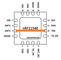
Product spec for nRF21540 reads “Control interface via I/O, SPI, or a combination of both” – I think that means, I can
use SPI bus exclusively for accessing All of the 21540 functions – i.e. no I/O needed, except for PDN (and SPI CSN)?
If so, how are unused nRF21540 pins 4, 7, 8, 9 supposed to be terminated – left unconnected, tied to VDD, or GND?

In may case "SPI-only" interface (no I/Os needed) is convenient for sure. But in your experience/ opinion, is there any
potential downside, such as performance and/or (OS/ driver/ example code) support penalty in taking this route?

Please advise. Thanks.

Parents
  • Hi,


    You can use SPI for control, but there will be a write delay so for real-time operation you should use GPIO control. In this case, the TX_EN and RX_EN pins should be tied to ground. The driver is still in the works so for now I would maybe recommend adding all pins, just in case.


    Best regards,
    Andreas

  • Thanks Andreas,

    Another question as I am wrapping up the design, will share for review shortly.

    I am trying to create a configuration where nRF21540 may be BOM called for optional assembly.
    For the assembly that doesn't require FEM - trying to come up with a best way to bypass FEM - 
    effectively connecting pads 10 and 3 of nRF21540 footprint. Of course, in way that won't impact
    RF performance in any adverse manner.

    Please advise what would be the best way that you recommend to effectively bypass nRF21540

  • Hi,


    I would avoid routing and thus changing the layout underneath the nRF21540. This will cause mismatch and/or alter the grounding of nRF21540 while that is assembled, which should be avoided to minimize the risk of any surprises down the road.

    I would add a transmission line around the device, something like this:

    This way you would mount the two green caps instead of C1 and the new blue cap, to disconnect nRF21540 without any shunt stubs in the RF line. Similarly, if nRF21540 is mounted, the bypass path will not introduce any shunt stubs, the blue cap must still be mounted but if using a rather large value (~10pF or larger) it will not cause any mismatch.
    This obviously requires a 4-layer stackup, or more, as the RF paths must have solid ground underneath, the control lines for nRF21540 must then be routed at the bottom layer or similarly far down the stackup.


    Best regards,
    Andreas

Reply
  • Hi,


    I would avoid routing and thus changing the layout underneath the nRF21540. This will cause mismatch and/or alter the grounding of nRF21540 while that is assembled, which should be avoided to minimize the risk of any surprises down the road.

    I would add a transmission line around the device, something like this:

    This way you would mount the two green caps instead of C1 and the new blue cap, to disconnect nRF21540 without any shunt stubs in the RF line. Similarly, if nRF21540 is mounted, the bypass path will not introduce any shunt stubs, the blue cap must still be mounted but if using a rather large value (~10pF or larger) it will not cause any mismatch.
    This obviously requires a 4-layer stackup, or more, as the RF paths must have solid ground underneath, the control lines for nRF21540 must then be routed at the bottom layer or similarly far down the stackup.


    Best regards,
    Andreas

Children
No Data
Related