
Hi,
As discussed, the instructed PCB land pattern for nRF9160 is according to Product Specification:
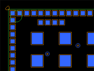
However, we have noticed that land pattern exceeds nRF9160 dimensions by ~0.5mm in DK (picture and gerber files):
Why extended land pattern is used in DK? Do you recommend this DK land pattern to be used in customer applications?
Br,
Juha
ps. I commented this already in December 2020 in some old thread but not sure if somebody reads it...

