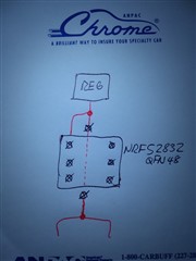
I'm designing a two layer board. I need to route the power supply to several parts while avoiding cutting up the ground plane. I'm consider running the power line on the opposite side of the board from a QFN NRF52 part. I will still have heat vias on either side of the VCC trace. Please take a look at my rough sketch. The red line is VCC which branches at the bottom to several other parts. The QFN pad will be solder on the top layer ground fill. Will this cause any problems either with the NRF part or with noise on the VCC line?