This post is older than 2 years and might not be relevant anymore
More Info: Consider searching for newer posts

The recommended PCB layout of nRF5340

Hi Sir,

As we know the nRF5340 doesn't release the Circuit Board Guidelines (nAN-40) like nRF52840 yet.

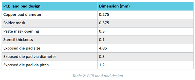
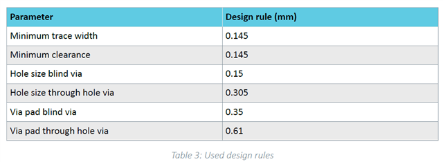
If we need to design the nRF5340, could you share the recommended PCB layout (or PCB land pad design) of nRF5340 for board design first?

Thank you.

BRs, Han

Parents Reply
  • Hi Hanyu

    I've asked for the numbers, but we don't have the updated document yet. 

    I've taken some measurements from the nRF5240 reference design:

    Copper pad diameter: 0.225 mm

    Paste mask opening: 0.327 mm

    Stencil thickness 0.1 mm

    Exposed die pad size: 5.4 mm x 5.0 (see the mechanical specification)

    Exposed die pad via diameter: 0.3 mm

    Exposed dia pad via picth: 1.333mm

    Min. trace width 0.125 mm

    Min clearance: 0.1 mm

    Hole size blind via 0.1 mm

    Pad size blind via: 0.3 mm

    Hole size through hole via 0.25 mm

    Pad size through hole via: 0.5 mm

    The two last are optional but this is what's used in the ref design. 

    Cheers,

    Ketil

Children
No Data
Related