This post is older than 2 years and might not be relevant anymore
More Info: Consider searching for newer posts

Clarify flash storage start & end address for nRF52840

I am using flash_fstorage_s140_pca10056 example from SDK v17.0.2, I see that the start address is 0x0003 E000 and the end address is 0x0003 EFFF respectively.

I want to determine the max size to store device configuration. This will let us decide limits on the data structure for storing device configuration. I have followed some of the threads on this topic and need some help in understanding the start and end addresses.

I have made no other changes to the code in the example project, I have only done the following change to print the end address. The value I get on logging is 0x00100000. In the following line, I determine the start address which is commented, I think that's not right. Need help here.

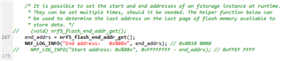
I haven't programmed any bootloader, I have erased the device fully and reflashed the binary. With reference to this thread, the value I get for NRF_UICR->NRFFW[0] is 0xFFFF FFFF. So, what's the start address in this case? I am confused with the values 0x0003 E000 and 0xFFEF FFFF.

Parents
  • Hi Jaimin, 

    Yes, you are correct on how to find the area between the end flash (can be the actual end of the chip's flash or it can be the last address before the bootloader start). 

    But be aware when you use the address right after the CODE_END, it's because the chip manage the flash by pages. So if you want to erase a word in a page you would need to erase the whole page. 
    So if you want to use the free space to store your application data, you should start from the next available page, not at CODE_END + 1

    Same applied for the last page. 

    Note that if your application use fds (which used in our BLE example) you need to avoid the area occupied by the fds module. 


    Hi Hung,

    Thank you for your response. I will ensure to not use CODE_END + 1 and instead use the next available page.

    Regarding FDS:

    I have not used the FDS module yet but I have skimmed through the flash_fds example project and fds.h file, I could not find specific information on the area occupied by the FDS module.

    Do you mean the reserved area by using fds_reserve API?

Reply
  • Hi Jaimin, 

    Yes, you are correct on how to find the area between the end flash (can be the actual end of the chip's flash or it can be the last address before the bootloader start). 

    But be aware when you use the address right after the CODE_END, it's because the chip manage the flash by pages. So if you want to erase a word in a page you would need to erase the whole page. 
    So if you want to use the free space to store your application data, you should start from the next available page, not at CODE_END + 1

    Same applied for the last page. 

    Note that if your application use fds (which used in our BLE example) you need to avoid the area occupied by the fds module. 


    Hi Hung,

    Thank you for your response. I will ensure to not use CODE_END + 1 and instead use the next available page.

    Regarding FDS:

    I have not used the FDS module yet but I have skimmed through the flash_fds example project and fds.h file, I could not find specific information on the area occupied by the FDS module.

    Do you mean the reserved area by using fds_reserve API?

Children
  • Hi Jaimin, 

    The FDS module uses fstorage as the backend to manage flash. It register the flash location that it occupies in flash_bounds_set() function. Basically it's located at the bottom end of the flash, either right before the bootloader, or right before the end of the physical flash if there is no bootloader. The number of pages it occupies is depends on the configuration , FDS_PHY_PAGES.

Related