
Dear Members,
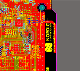
Where can I download altium antenna footprint for nRF52840 ?
Which file ? what's the name of that footprint ? thanks
Dear Members,
Where can I download altium antenna footprint for nRF52840 ?
Which file ? what's the name of that footprint ? thanks
I can't find it on altum hardware files,

I dont think we have just the pcb trace antenna as a component for download, but if you have downloaded the Altium board file then i belive that all you have to do is mark the antenna and copy or drag and drop to a different Altium pcb file and it will show up.
Regards,
Jonathan
I dont think we have just the pcb trace antenna as a component for download, but if you have downloaded the Altium board file then i belive that all you have to do is mark the antenna and copy or drag and drop to a different Altium pcb file and it will show up.
Regards,
Jonathan
I have added the PCB trace antenna copied from the ref design here:4375.PCB_trace_antenna.PcbDoc

Thanks for the reply,
on PCA10056-nRF52840 MCU Schematic Page,
Is it possible that I change the size all of the capacitors and inductors to 0805 ?
There are some 0402, which are difficult to hand soldered and twizered.
Thanks
Hi,
So a couple of things to
For the radio:
There are two things that we achieve with the components on is matching and the other is filtering harmonics. The first one, matching the impedance, is not that senestive to change in component size so going from a 0402 to 0603 or 0802 does result in huge changes when its the capacitors at least. For the harmonic filtering its another story, the change in size can/will have a huge impact on the results. The capacitors is less prone to impact the result as much as inductors so its definitely a safer way to test.
So for the capacitors(red) closest to the radio, should not be changed.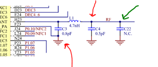
What you can do if you are able to test in house is make the pads on the PCB bigger in size so that they can accommodate both 0402 to 0802.
If are going to go up in size then try to leaf C3 alone.
The rest are not that sensitive so it should be fine, but i do recommend to sticking to the reference as closely as possible. And keep the specs equal or better on the components you change size on if you want the best performance.
But when it comes to hand soldering small components a god sett of twizers and propper support for your arms/elbows goes a long way when placing and soldering the components, and some magnification is always helpful.
PS: we do HW review so if you want your schematic\layout reviewed you can create a new public or private case hare on Devzone and we will address it.
Regards,
Jonathan
PS: we do HW review so if you want your schematic\layout reviewed you can create a new public or private case hare on Devzone and we will address it.
I have a schematic and PCB layout, how can I open a private case ?

Hi,
I will cover for Jonathan, he is out of office today.
You go to tech support on DevZone, press the bottom " + New", chose "PRIVATE Tech Support" and fill out the ticket:
Best regards,
Kaja