
I'm designing the nRF52840 into a new product with BLE, LTE and GPS.
Could you please point me to a recommended matching network and antenna solution for the nRF52840?
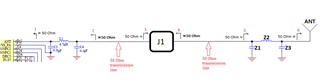
We will use a 2:1 MUX to select between a board mounted antenna and external antenna connector. So there must be AC coupled 50Ohm nodes at the mux input and outputs.
The internal antenna could be PCB type or an SMD component. I don't have a preference.
Should I use a SAW filter in this setup?
I may have access to a VNA. What would be the best method to tune the antenna? With our without the radio mounted?
In the board stackup I can have the reference ground plane either 0.1mm or 1.5mm below the RF signal layer. This is a 4L stackup with microvias. The outer insulation layer thickness has a fairly large tolerance. I plan to use L3 as ground reference to allow for a few non-critical signals routed on L4. The question is whether I should use the much nearer L2 as ground reference as well.
Best regards,
Børge

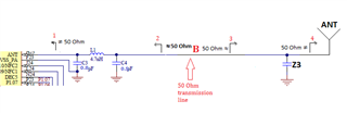
 (J1 is a RF test connector, not required)