This post is older than 2 years and might not be relevant anymore
More Info: Consider searching for newer posts

Help needed with NRF24 reference design

Hi

I'm relatively new at pcb design, and have been trying to create my own designs fully assembled with SMT as opposed to just creating a soldershield. I'm making a wireless receiver device and have tried a design with a mifa (?) antenna before, which failed miserably. I was adviced to follow the reference design which I think I did in this one, albeit I get even poorer or none working signals with this:

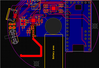
With the mifa antenna I was getting signals, but muddy and with a lot of noise. With this one I am not able to get any so I am assuming there is a big flaw, but I cannot spot it when comparing my nrf24l01+ layout to the reference design? Any help or advice on how to toubleshoot would be appreciated.

Tia,

Bob

Parents
  • You need ground planes on both sides, connected with plenty of vias. The area under the matching network should be solid ground. Route as much as you can on the top layer to make the bottom layer a good ground plane. 

    The antenna doesn't necessarily needs to look like this. It's just a simple 1/4 wave track. So you can make it a straight track instead. It's more important to keep it away from any metal. 

Reply
  • You need ground planes on both sides, connected with plenty of vias. The area under the matching network should be solid ground. Route as much as you can on the top layer to make the bottom layer a good ground plane. 

    The antenna doesn't necessarily needs to look like this. It's just a simple 1/4 wave track. So you can make it a straight track instead. It's more important to keep it away from any metal. 

Children
Related