
I am currently working on an application running on the nRF52 DK which will use some inputs and output to interface with the environment. Its a BLE application and those inputs will be used to trigger some actions (input signals) or interface via SPI to the outside (OLED display, output signals).
I am unsure which pins/GPIOs are already claimed by DK onboard hardware and which are really free to use.
Please notice that I do not want to physically modify the DK at all. So cutting traces or anything to free a GPIO is not an option. I explicitly want to know which pins are free per design.
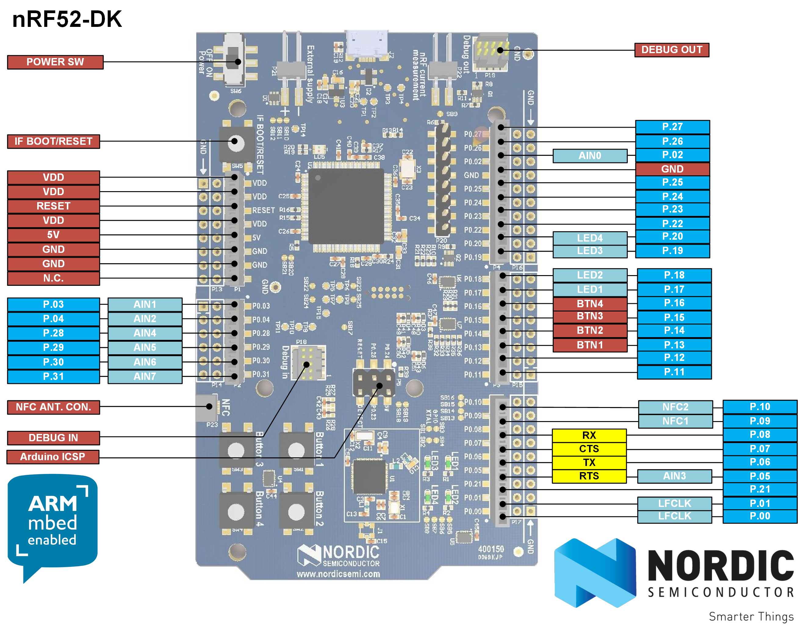
Using the nRF52 DK pinout reference at: https://os.mbed.com/media/uploads/andrzej_z_krakowa/nrf52_dk_pinout_armmbed_enabled_v2.png
Currently I am using in my application:
P0.11, P.12,
P0.22, P0.23,
P0.24, P0.25, P0.26, P0.27,
P.31
The GPIOs for the LEDs and On board buttons from the BSP (P0.13-P0.20) are also in active use.
I am unsure about the following pins:
* P0.0, P0.1: LFCLK == Low frequency clock? Is this in use per default in a BLE application or can I use those? I am currently using application timers in my code. (As an input or output)
* P0.2, P0.3, P0.4, P0.28, P0.29, P0.30 (these are all labeled as AINx - but I am already successfully using P.31 from that bank (as an output), so I presume it should be no problem to use those?) (as input or output)
* P0.9, P0.10 - I am not using NFC in my application so I presume those are free to use as well and are not pre-occupied/blocked by the NFC on-board connector? Can those be used as input/output?
* P0.5, P0.6, P0.7, P0.8 - those are associated with UART in the pinout picture. I am not actively using UART - is this potentially in use by the Segger debugger or can I use those as well? (For input/output)
The current application used P0.26 and P0.27 for TWI/i2c so far. I also tested some SPI using those pins as CLK and DIN (and P0.11, P0.12, P0.31 for the rest). It's not yet 100% clear if I will use TWI or SPI in the end. Am I completely free in choosing my pins for SPI? I think P0.3, P0.4, P0.28, P0.29, P0.30 and P0.31 might be a good candidate as they are all next to each other. Can I use/configure SPI with those or is P0.26 and P0.27 mandatory for CLK and DIN so I would have some pins here and some there?
Thank you very much!
