
I'm kind of confused about the DCDCEN0/1 related functionality and can use some confirmation. If I'm hoping to run everything at 1.8V, it seems I can wire VDD_NRF to 1.8V and then expect all my GPIO to operate with a VDD_high of 1.8V. Is that correct? Does that mean I can just ignore high voltage mode and the DCDCEN0/1 blocks?
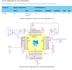
In terms of wiring the nrf52840 on my PCB, does that mean I could use config 3 from the datasheet (screenshot below)? From my understanding, this should work fine on startup and not limit my SPI read/write rate or my BLE functionality.
https://infocenter.nordicsemi.com/index.jsp?topic=%2Fps_nrf52840%2Fref_circuitry.html&cp=4_0_0_6_2
Big thank you to anyone who can help!
Kindest regards,
Ryan
