Hallo everyone,
nrf52840 Dk (Master device)
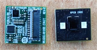
MAX86140 (Slave device)
I have been working with an AFE (Analog front end) sensor recently. It is a 19 bit charge ADC with dedicated LED driver. This is the link to the datasheet.
Even though I was able to write data to the register, I am finding it difficult to read data from it. There is no or too little (unexpected) activity in the MISO line. While all other lines functions as expected.
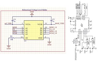
There is a logic level shifter since the AFE works with 1.8 V logic. I am using TXB0304 from TI as a logic level shifter.
I am using Mode 0, 125K clock frequency (Even though MAX86141 supports 4M Hz. Writing is also possible with high clock rates )
Datasheet says "Data is strobed into the MAX86140/MAX86141 on the SCLK rising edge while clocked out on the SCLK falling edge. All single-word SPI read and write operations are done in a 3-byte, 24 clock cycle SPI instruction framed by a CSB low interval."
This is the timing diagram. This details can be found on datasheet page number 52.
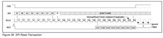
The AFE consist of a 128 byte FIFO for storing the digital data. The FIFO is burst read each time. But here I am trying to read a single register (Register Part ID (0xFF)), which should return a hex code of 0x24 according to datasheet (Page 86 of datasheet). The datasheet says, "Configuration and status registers are available through normal mode readback sequences."
Following are the functions used for read and write.
#define WRITE 0x00
#define READ 0xFF
#define SPI_BUF_SIZE 3
#define SPI_INSTANCE 0

static uint8_t m_tx_buf[SPI_BUF_SIZE];
static uint8_t m_rx_buf[SPI_BUF_SIZE];
static const uint8_t m_lenght = sizeof(m_tx_buf);
uint8_t value;
volatile uint8_t SPIReadLength, SPIWriteLenght;


void MAX86141_reg_write(uint8_t addr, uint8_t data_in)
{

  SPIWriteLenght = 3;
  SPIReadLength = 0;

  m_tx_buf[0] = addr;
  m_tx_buf[1] = WRITE;
  m_tx_buf[2] = data_in;

  m_rx_buf[0] = 0;
  m_rx_buf[1] = 0;
  m_rx_buf[2] = 0;


  //NRF_LOG_INFO("Starting to write data \n");
  APP_ERROR_CHECK(nrf_drv_spi_transfer(&spi, m_tx_buf, 3, m_rx_buf, 0));

  while(!spi_transfer_done);
  //NRF_LOG_INFO(" Transfer success! \n");

}

void MAX86141_reg_read (uint8_t addr, uint8_t *data_out)
{
   m_tx_buf[0] = addr;
   m_tx_buf[1] = READ;
   m_tx_buf[2] = 0x00;


   m_rx_buf[0] = 0;
   m_rx_buf[1] = 0;
   m_rx_buf[2] = 0;

   spi_transfer_done = false;
   APP_ERROR_CHECK(nrf_drv_spi_transfer(&spi, m_tx_buf, 3, m_rx_buf, 3));

   while(spi_transfer_done == false){};

   *data_out = m_rx_buf[2];
   //NRF_LOG_INFO("Inside the read function. Value is :%d", m_rx_buf[2] );
}
spi initialisation .
static const nrf_drv_spi_t spi = NRF_DRV_SPI_INSTANCE(SPI_INSTANCE);
static volatile bool spi_transfer_done;


void spi_event_handler(nrf_drv_spi_evt_t const *p_event, void *p_context)
{
    spi_transfer_done = true;
    if (m_rx_buf[0] != 0)
    {
        NRF_LOG_INFO(" Received:");
        NRF_LOG_HEXDUMP_INFO(m_rx_buf, m_lenght);
        NRF_LOG_FLUSH();
    }

}

void spi_init()
{
  nrf_drv_spi_config_t spi_config = NRF_DRV_SPI_DEFAULT_CONFIG;
  nrf_drv_spi_frequency_t frequency;
  spi_config.ss_pin   = MAX86141_CS_PIN;
  spi_config.miso_pin = MAX86141_MISO_PIN;
  spi_config.mosi_pin = MAX86141_MOSI_PIN;
  spi_config.sck_pin  = MAX86141_SCLK_PIN;
  spi_config.mode = NRF_DRV_SPI_MODE_0;
  spi_config.frequency = NRF_SPI_FREQ_4M;
  APP_ERROR_CHECK(nrf_drv_spi_init(&spi, &spi_config, spi_event_handler, NULL));
}
Spi pins used:
// SPI pins

#define MAX86141_CS_PIN 31
#define MAX86141_MOSI_PIN 29
#define MAX86141_MISO_PIN 30
#define MAX86141_SCLK_PIN 26
In the main function,
int main(void)
{

loginit();
NRF_LOG_INFO("Program Started");

uint8_t value = 0;
spi_init();
NRF_LOG_INFO("Initializing SPI \n");

nrf_delay_ms(200);
MAX86141_init();


    while (1)
    {
MAX86141_reg_read(REG_PART_ID, &value);
nrf_delay_us(1);
   }
}
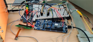
These are the signals from a logic analyzer. If the images are not clear, please let me know. ( Its a very old logic analyzer from 90s).
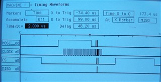
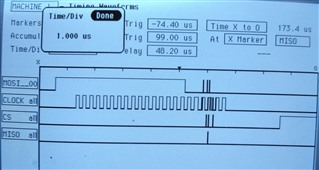
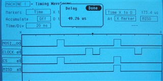
As mentioned, I am trying to read data from register Part ID (0xFF). So according to the SPI timing diagram, the first byte in the MOSI line is the address (11111111), the next is a read command which is 1 bit ( I am sending 1 byte 0xFF. the rest 7 bits are ignored), now for the last 7 bits, I am expecting 0x24 (0010001) from MISO line. As you can see from the above three figures (which are same but enlarged), the lines experiences heavy glitches for the last 7 clock signals. The values read are garbage data. This has been the issue for the past two weeks.
I am using the sensor module from the MAX86140 Evaluation Board. So I am using a FPC to DIP convertor and accessing the SPI pins from the sensor directly. The two LEDs in the evaluation sensor mode makes it easy to confirm that the registers have been written.
Following tasks were performed to figure out the problem.
1. The signal MISO line from the sensor was directly probed, rather than letting the signal pass through the level shifter. The same fluctuations in the signal line were noticed even for the signal coming out from the sensor end.
2. SPI pin connections were crossed verified for any errors.
3. The sensor is working and is able to read data using the evaluation board. It comes with a GUI were the data can be read and written in to.
4. Clock, CS and MOSI lines are showing expected values when decoded using a level shifter (As shown in the figure above)
5. Clock rates were varied. 125K to 4M. But this does not solve the issue.
I kindly request help from your side. Any suggestions will be accepted.
Thank you for your time.
Best Regards,
Karlz