Hi Nordic,
Please, I am doing a design with nRF52840 and would like to be clear on a few points. Attached is the electrical diagram .
Point 1
For the power supply I am using a schematic as shown in figure 16 (page 63) of the datasheet and also used in the nRF52840 Development Kit. Hi Voltage Mode, DC/DC for REG0 and REG1 enabled.
In this scheme the power input is 3.3V on VDDH (only this pin Y2), while all the VDD pins are power output from the nRF52840. I am not using VDD to power any other circuitry external to the nRF52840.
1-) Is this correct? Just have the VDDH pin (Y2) as power input.
2-) According I understood with this power supply topology the DIO voltage levels can be configured. Am I right?
3-) I need to use two independent UART interfaces, can I set the voltage level on one interface to 1.8V and on the other interface to 3.3V? Or both UART interfaces must work at the same voltage level (3.3V preferably)?
Point 2
In my application I need to use two independent UART communications, as I read in the datasheet the UART signals can be routed to any DIO pin.I named each interface UARTA and UARTB. So I have connected
UARTB_TX -> P0.30 (B9)
UARTB_RX -> P0.28 (B11)
UARTA_TX -> P0.29 (A10)
UARTA_RX -> P0.02 (A12)
UARTA__CTS -> P1.15 (A14)
UARTA_RTS -> P1.13(A16)
1-) Are the connections correct?
2-) Can I use two independent UART interfaces without shared resources conflict?
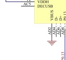
Point 3
1-) If the USB interface is not used, can the USB pins be left open?
Point 4-)
On pin 1 of the programming connectors (debug in and trace P18, P25), what should I connect VDDH or VDDD?
Atthached the shematic.
Sincerely thank you very much. Best regards