Hello,
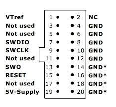
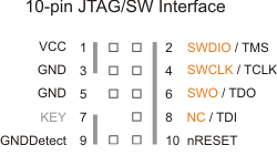
My goal is to use the Jlink JTAG for programming custom nRF52 boards (specifically, nRF52840) using minimum number of wires. The default Jlink JTAG is a 20pin connector, or it can be reduced to 10 pins using an adapter. From what I read, all I need is a connection from VCC (aka VTref), GND, and SWDIO and SWCLK to my custom board. However, I've been getting errors saying that my Jlink cannot recognize the board.


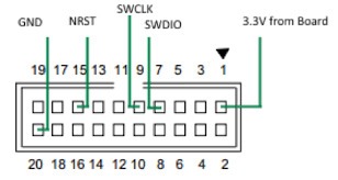
For example, my hookup follows the below (I am not using pin NRST, tho). I am using male jumper wires from the JTAG onto my board. I get this error from the Segger J-Flash Lite software when I attempt to flash new firmware. I've tried multiple placements of the GND pin, but nothing.

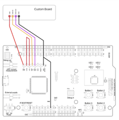
I tried programming the nRF52840 PCA10056 board using this method as a sanity check, and still, board not detected. Here's an example wiring diagram I took online, which I thought would work; in this case the VTG and GNDdetect are shorted to VCC and GND, respectively, and the custom board is actually my Jlink device feeding in the SWD signals for programming.

My goal is to build around the JLink and create a programming fixture using pogo pins to program our boards at production. Our boards only expose GND, VCC, SWDIO, and SWDCLK. Once a bootloader is flashed, we'll program normally through USB.
Best,
George


