This post is older than 2 years and might not be relevant anymore
More Info: Consider searching for newer posts

How to control the sclk in spi communication to perform offset calibration while using nRF52840 dongle with ADS1234IPW.

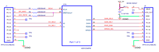
Respected Sir/Ma'am,

I have attached my schematic below.

I need to perform Offset calibration operation for which I need to control the SCLK value.

I am sending a 24 bit clock to get my output data value which is 3 byte.

how can pass 2 more clock cycles to to perform the offset calibration.

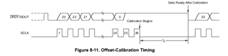
Is there any function for the same.

Or could you suggest me how I could code for it.

Parents
  • Have you tried sending an empty 4th byte? ie a 4 byte transfer.

  • hello sir,

    Well sending a 4th byte would not be a correct option for this as I have to send only 26 bits clock cycle so that at the falling edge of the 26th clock cycle the offset error calibration should begin.

    so could you please let me know how can I send 2 extra bits.

  • Actually you can simply send a 4th byte with no measurable degradation:

    "Offset calibration can be initiated at any time to remove the ADS123x offset error. To initiate offset calibration, apply at least two additional SCLKs after retrieving 24 bits of data. Figure 8-11 shows the timing pattern. The 25th SCLK sends DRDY/DOUT high. The falling edge of the 26th SCLK begins the calibration cycle. Additional SCLK pulses can be sent after the 26th SCLK; however, minimize activity on SCLK during offset calibration for best results"

    Since calibration takes 100mSec (80ssps) or 800mSec (10sps) I think the noise period for the extra 5 clock cycles at (say) 4MHz can be safely ignored. The best way to minimise noise during offset calibration is to ensure the nRF52 remains asleep.

    Very nice noise figures for this chip.

Reply
  • Actually you can simply send a 4th byte with no measurable degradation:

    "Offset calibration can be initiated at any time to remove the ADS123x offset error. To initiate offset calibration, apply at least two additional SCLKs after retrieving 24 bits of data. Figure 8-11 shows the timing pattern. The 25th SCLK sends DRDY/DOUT high. The falling edge of the 26th SCLK begins the calibration cycle. Additional SCLK pulses can be sent after the 26th SCLK; however, minimize activity on SCLK during offset calibration for best results"

    Since calibration takes 100mSec (80ssps) or 800mSec (10sps) I think the noise period for the extra 5 clock cycles at (say) 4MHz can be safely ignored. The best way to minimise noise during offset calibration is to ensure the nRF52 remains asleep.

    Very nice noise figures for this chip.

Children
Related