This post is older than 2 years and might not be relevant anymore
More Info: Consider searching for newer posts

NRF52832 hardware design evaluate

Hello, 

  We are using NRF52832 to design a loss  preventer    product ,can you help to review the design SCH and PCB layout  before PCBA making ? main including  RF desing , GPIO  using , crystal choosing ,  programming  and PCB layout etc. hardware issue .attached is the schematic and PCB.pls kindly provide your suggestion.

 T10-00499-XX REV00 SCH&PCB 20210521.pdf

Parents Reply Children
  • Hi,

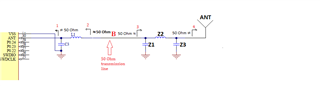
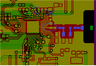
    1. The RF path should be directly copied from the reference layout, placement of components, traces.. the blue trace should be a 50 Ohm tranmssion line, a coplanar waveguide. 
    2. Avoid routing under the traces to the crystal, to avoid noise on the clock and radio. 
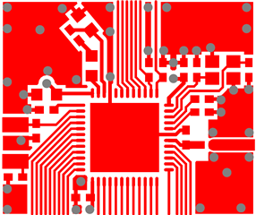
    3. C6 and C33 should be placed close to pin P0.25 and P0.26 as in the reference layout, to reduce the noise and work as a sufficient workaround for errata 138. 
    4. I can't see any drill holes in this gerber folder.. could you share a picture of the top layer with drill holes? 
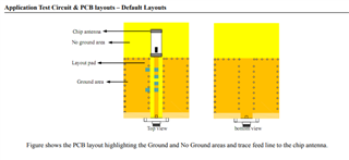
    5. The antenna is an pcb end mounted antenna, here it's mounted as a center-edge mounted antenna.. and the antenna pad closes to the radio is placed within the ground area, blocking it in even more.. I would recommend that you talk to the antenna vendor, and see what they say about this layout, you might have to consider changing the antenna, most vendors has a selection guide, like this one. 


    Best regards,
    Kaja

Related