This post is older than 2 years and might not be relevant anymore
More Info: Consider searching for newer posts

Where can I find EAGLE library for nRF52840-CKAA-R WLCSP-93 package?

samuelbaldwin

Hello,

Does anybody know where I'll be able to find an EAGLE library for the nRF52840 CKAA chip (the WLCSP-93 package)? I've looked around and all other dev boards that have their libraries available all use the 7mm x 7mm QIAA version. This is way too big for the product I'm designing so I need the 3.6mm x 3.6mm smaller package.

Parents Reply Children
  • Hi,

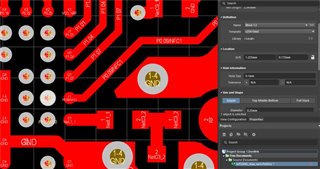
    The Gerber files for the CKAA WLCSP package is available here. See the production files folder. 

    regards

    Jared 

  • hey thanks a lot Jared! that was Really helpful.


    We have a follow up query on this, would be able to assist us with the same?

    based on this package type,  while routing our engineer noticed we will need a via of 0.05 mm. We don't know any pcb fabricator with such capabilities.

    Would you be able to support us with any contact or a work around?

  • Hi.

    Exactly what vias are you thinking about? In any case, it would be wise to contact the pcb production house and ask them what they would advise using instead.

    And this is a recommended read. 

    regards

    Jared 

  • Hey Jared.

    So basically our team has done the routing based on the above recommendations, but we are unable to find a production house that has the capabilities to support our requirement. 

    We basically making a really small PCB. can you support us with this information:?

    1. Via hole dimension,(in our case we need to go for both blind and burried via's since our pcb size is small)
    2. pad to pad clearance trace width

    ( for nRF52840-CKAA-R WLCSP-93 package.)

     All the production houses we have reached out to support a minimum track and gap of 0.075mm and a laser drill of 0.1 mm .  Have we overlooked something? Any suggestions on how my team can move pass this impasse would be great! 

  • Hi,

    The minimum via size that is used in the reference design is 0.1 mm:

    Even though your design is small I would think it would be possible have the same size vias? Have you seen our nRF52840 dongle designThe pad to pad clearance trace width is entirely dependent on the production house used. It doesn't seem like this would be an issue in your design. I also suggest that you create a new private ticket for a HW review. There is several things of concern in your design, proper grounding for instance. Attach your schematic and PCB hw files in a new ticket for a HW review. 

    regards

    Jared

Related