

Hello!
Sorry in advance for what is probably a very simple mistake. I am currently trying to develop a simple PCB for the nRF5340 QKAA aQFN94 package using EasyEDA (bare minimum, mostly the reference circuitry from example no. 4). I have had no issues with the schematic, however I have run into issues routing all the pins from the package. In the PCB layout example, it shows routing going in between pins, along with pins being accessed through mid-layer 1. Using the minimum routing and spacing supported (0.0889 mm), my traces cannot fit in between pins, and the minimum size vias (0.2mm holes, 0.4mm diameter) is far too large to put near or on any of the pins to access other layers. The only clue that I have right now is in the nRF52840 whitepaper, where it uses microvias, but I'm not seeing anything that shows those are supported by many PCB manufacturers. Please let me know if I am doing anything wrong and how I can fix these issues. If any further detail is needed, please ask.
Showing minimum trace width: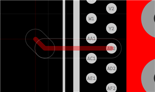
Showing minimum via size: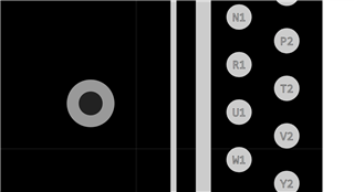
Thanks in advance,
Andrew
