This post is older than 2 years and might not be relevant anymore
More Info: Consider searching for newer posts

Antenna not working with BAL and 2450AT18B100E

Hi Everyone

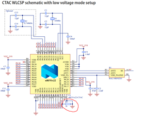
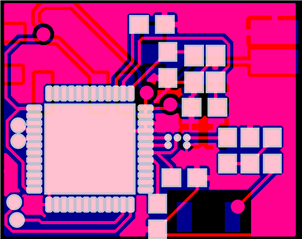
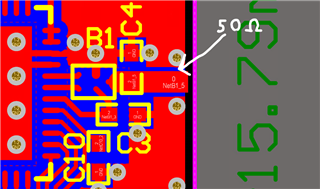
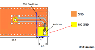
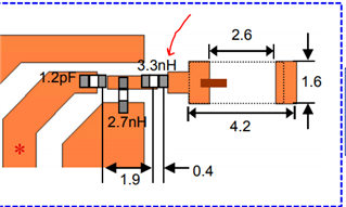
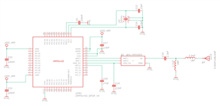
This is my first time designing a PCB with the NRF51822. I have designed it using an 2450AT18B100E Antenna and a BAL-NRF02D3 balun. Below is my schematic:

 (Click on the image to enlarge it)

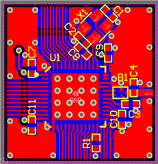
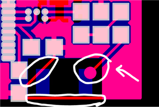
After assembling the PCB, everything seems to work apart from being able to see/connect to the BLE device. I am using "NRF Connect" app on my device to scan for it but nothing shows up. I then transferred the NRF51822 from my custom PCB above PCB to the NRF51822 development board and it works fine, so I know the code is good. I'm just not sure where I have gone wrong with my PCB design causing the BLE to not show.

Is anyone able to spot something wrong with my schematic that I may have missed? 

Cheers
Joel

Parents
  • Hi, 

    I cant see any obvious errors in the schematic. Could you share the Layout files(in GERBER )? 

    One thing that might be the issue is not properly loading the crystal, so can you just confirm that you have used the 12pF on X1 ?


    Only comment on the schematic is that you should have a pulldown on SWDCLK in case there is a abundance noise then the chip might end up in debug mode. 

    But that is probably not the reason you dont see any radio activity. 

    Regards,
    Jonathan

  • Hi Jonathan

    Thanks for taking the time to reply. Attached is the Gerber files and inside that is an updated schematic for this specific board.

    Keep in mind I only need BLE to work for a maximum of 1 meter. Also I have tried attaching the antenna hanging off of the PCB with a wire, but still didn't make a difference

    Link to Gerber files: mega.nz/.../4WgzWSzL
    (I could not find a way to attach the files directly, so I had to upload them to mega

  • Hi,

    I am not bale to access mega.nz for some reason, could you try to re upload the files?


    If yo first make a folder and call it GERBER, then add all the gerber files in that folder. Zipp that folder, once the folder is zipped you can try to re upload it here on Devzone.


    Klick on Insert, then select image/video/file


    Then click the upload and select the zipped file


    Regards,
    Jonathan

  • Thanks for showing me how to do it. I have attached the files here now.NRF51822_help.zip

  • Thanks,


    I see som issues here related to the RF layout that is causing the poor performance/ not working properly. 

    I am not sure that it is possible for that design to work as you hope, and would suggest that you do a redesign of the PCB, focusing on the radio part. 


    Here is the reference layout of the nrf51822:


    And this is your design


    There is quite the difference in layout, on thing that is important is to follow the layout closely to get a ok performance. 
    The output from the balun should be a 50 ohm impedance line, and here is where you should place the pi-matching or T-matching network.


    If we look at the antenna datasheet for the 2450AT18B100E wee se that there is some references to follow as well. 

    The yellow area is importen to keep clear of any GND, and that applies for all layers of the PCB. 

    The arrow points at the feed line to the chip antenna and it should ideally be as close to the last series component, and the other circles are traces that cross the area of the keep out area for the antenna to work as intended. 


    It is hard to say if there is only a singel source for the problem here, i belive there are many factors that results in the radio not working as intended in this case. 


    I think you have to re-design the PCB to better accommodate the needs of the antenna and radio to have a successful device. 

    Regards,
    Jonathan

Reply
  • Thanks,


    I see som issues here related to the RF layout that is causing the poor performance/ not working properly. 

    I am not sure that it is possible for that design to work as you hope, and would suggest that you do a redesign of the PCB, focusing on the radio part. 


    Here is the reference layout of the nrf51822:


    And this is your design


    There is quite the difference in layout, on thing that is important is to follow the layout closely to get a ok performance. 
    The output from the balun should be a 50 ohm impedance line, and here is where you should place the pi-matching or T-matching network.


    If we look at the antenna datasheet for the 2450AT18B100E wee se that there is some references to follow as well. 

    The yellow area is importen to keep clear of any GND, and that applies for all layers of the PCB. 

    The arrow points at the feed line to the chip antenna and it should ideally be as close to the last series component, and the other circles are traces that cross the area of the keep out area for the antenna to work as intended. 


    It is hard to say if there is only a singel source for the problem here, i belive there are many factors that results in the radio not working as intended in this case. 


    I think you have to re-design the PCB to better accommodate the needs of the antenna and radio to have a successful device. 

    Regards,
    Jonathan

Children
No Data
Related