This post is older than 2 years and might not be relevant anymore
More Info: Consider searching for newer posts

PCB Design Altering the nrf52832_ciaa reference

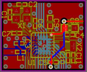
I'm planning to modify the nrf52832_ciaa reference designs in altium to emulate the functionality from a development kit and add an RTC. 

I need access to pins P0.23, P0.22, P0.14, as well as SWDIO/SWDCLK for programming/debugging.  Can I directly route the traces for these pins as needed to connect the RTC and add output pads for the SDWIO/SWDCLK?

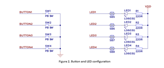
I wanted to clear up this paragraph from the datasheet: "The buttons are active low.... The buttons have no external pull-up resistor, so to use the buttons the P0.13 – P0.16 pins must be configured as an input with an internal pull-up resistor."  Does this mean that in the software I can configure P0.14 with an internal pull-up resistor, then just connect a switch across P0.14 that grounds when connected to make this work?  I prototyped this with the nrf52DK and had to add an external circuit that connects to 3.3V with open switch and gnd with closed switch and I assumed I would have to add this circuit to the PCB, but the datasheet paragraph I quoted makes me think otherwise.  Could someone clear this up?

I also wanted to add an external 3.3V coin cell and was planning to place this on the bottom side of the board (side with no components in altium).  I see a pin labeled VDD_NRF so if I route the battery's output to this trace will this be sufficient to power all the components, or do I need to route to other places as well?

I also wasn't planning to change the antenna matching network capacitor/inductor since the only changes being made are adding an RTC and battery holder.  Is it reasonable to assume that this will still function properly, or will the matching network need to be recalibrated?

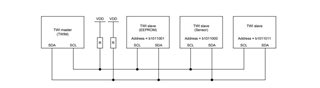
Lastly, I'm planning to use TWI to communicate with the RTC and found this diagram (attached below).  It has the SCL and SDA lines pulled up to VDD and I was wondering if this was done internally or if I would need to add this to the PCB.  

I bolded all my questions and just wanted validation for my plan of how to setup this PCB since I haven't worked with PCB design to this extent before.  The bolded questions are what I'm mostly concerned with, please let me know if you see any major issues/holes in my plan and understanding!  Thanks for the help!

Parents
  • Hi pardon the slow reply,

    First I just want to say that if you want us to look at the schematic and PCB layout of your project we can do that. Create a new Devzone ticket and call it PCB review (chip that you use), and if you want tit to be private then just crate a private ticket.  


    Can I directly route the traces for these pins as needed to connect the RTC and add output pads for the SDWIO/SWDCLK?

    If the plan is to use i RTC chip and interface to the nrf52 then usually TWI or SPI is used, in that case direct routing is ok for the GPIO's that you want to use. 
    As for the SWDIO and SWDCLK you can rout the trace to some pads or trough hole or a connector or what ever you like. 


    if I route the battery's output to this trace will this be sufficient to power all the components, or do I need to route to other places as well?

     
    It should be sufficient to connect to the VDD_nRF line with he battery. 


    Does this mean that in the software I can configure P0.14 with an internal pull-up resistor, then just connect a switch across P0.14 that grounds when connected to make this work? 


    Here is how it is done on the DK
    https://infocenter.nordicsemi.com/topic/ug_nrf52832_dk/UG/nrf52_DK/hw_btns_leds.html?cp=4_2_4_5_4 

    You don't have to use external circuitry. 


    Is it reasonable to assume that this will still function properly, or will the matching network need to be recalibrated?

     If you don't deviate to far from the reference layout then it will not need a recalibration and should work just fine. 


    Regards,
    Jonathan

Reply
  • Hi pardon the slow reply,

    First I just want to say that if you want us to look at the schematic and PCB layout of your project we can do that. Create a new Devzone ticket and call it PCB review (chip that you use), and if you want tit to be private then just crate a private ticket.  


    Can I directly route the traces for these pins as needed to connect the RTC and add output pads for the SDWIO/SWDCLK?

    If the plan is to use i RTC chip and interface to the nrf52 then usually TWI or SPI is used, in that case direct routing is ok for the GPIO's that you want to use. 
    As for the SWDIO and SWDCLK you can rout the trace to some pads or trough hole or a connector or what ever you like. 


    if I route the battery's output to this trace will this be sufficient to power all the components, or do I need to route to other places as well?

     
    It should be sufficient to connect to the VDD_nRF line with he battery. 


    Does this mean that in the software I can configure P0.14 with an internal pull-up resistor, then just connect a switch across P0.14 that grounds when connected to make this work? 


    Here is how it is done on the DK
    https://infocenter.nordicsemi.com/topic/ug_nrf52832_dk/UG/nrf52_DK/hw_btns_leds.html?cp=4_2_4_5_4 

    You don't have to use external circuitry. 


    Is it reasonable to assume that this will still function properly, or will the matching network need to be recalibrated?

     If you don't deviate to far from the reference layout then it will not need a recalibration and should work just fine. 


    Regards,
    Jonathan

Children
No Data
Related