Hi:
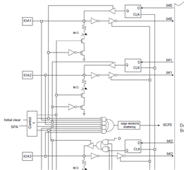
I want to know structure of nRF52810 GPIO. Also what's different structure bewteen output standard drive and output strength drive. where could I find these information.
Hi:
I want to know structure of nRF52810 GPIO. Also what's different structure bewteen output standard drive and output strength drive. where could I find these information.