Hello,
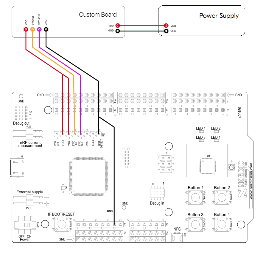
I want to program and debug a custom PCB using the nRF52832 SoC and nRF52 DK. I plan to use this setup:

From what I understand, the GND detect will cause the PCA10040 on the DK to subvert the nRF52832 chip on the DK and program directly to the nRF52832 chip on the custom PCB. Is this correct?
I was also wondering how to debug using this. Is it possible to use a terminal emulator such as putty to debug using this setup in the same way that putty would be used to debug the development kit? Or do I need to use a different method to debug?
Thanks!


