
Hello everyone
I'm doing my first steps so as to get things right from the start with a device based on the nRF52833 chip.
My setup: PC <USB> nRF52840-DK <JTAG> CustomBoard (nRF52833)
I am struggling to understand the TWI workflows and keep getting hard faults
Can one of you good people confirm or infirm the following points:
1) the functions nrf_drv_twi_tx or nrf_drv_twim_tx carry out an entire Master write sequence:
START, Address, 0W, (slave_ACK) - data[0] - (slave_ACK) - data[1] - (slave_ACK) .....- STOP
2) the functions nrf_drv_twi_rx or nrf_drv_twim_rx carry out an entire Master read sequence:
START, Address, 0W, (slave_ACK) - (slave_data) - NACK - STOP
3) To e.g. read a register, I have to write
- a tx function (sensor address, which register to be read)
- a rx function (sensor address, data from register defined in tx query)
Is this correct? In the sensor's datasheet (APDS-9603-065), the flow does not include a "break", i.e. NACK + STOP, for a register read.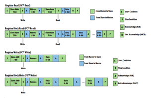
Thank you, in advance, for the precious help
Jerome
