This post is older than 2 years and might not be relevant anymore
More Info: Consider searching for newer posts

How to troubleshoot a chip antenna on custom PCB with 52832

Hello,

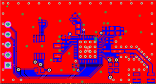
I have successfully programmed the ble_app_uart example to a custom PCB using the 52832.  Here is the board schematic, on the board C15 and C16 are not fitted.

2047.nrf52832_qfaaThirdRevision1.pdf

Using RTT I was able to confirm that the advertising start function started with an error code of 0, so I assume that the program is working as intended.  I am unable to find the device using nRF toolbox  to scan for BLE devices despite advertising, which makes me think there is an issue with the antenna.  

Here is the PCB document in altium:

4885.nrf52832_qfax_dcdcThirdRevisionRoutedEddieChangesNordicScott_20JUL2021.PcbDoc

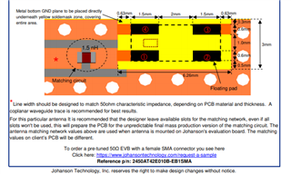
I used a coplanar waveguide calculator which said that the RF feed line should be 30mil to achieve a 50ohm impedance.  The antenna used is: https://www.digikey.com/en/products/detail/johanson-technology-inc/2450AT42E010BE/6235443 

Its datasheet is: https://www.johansontechnology.com/datasheets/2450AT42E010B/2450AT42E010B.pdf

I am working on figuring out what may be the issue here and any help would be appreciated.  Since the board was able to connect and program successfully the antenna seems to be the issue, but I wasn't sure if there were any measurements or things I could try to hone in on the problem further.  Thanks!

Parents
  • Hi Jake,

    some comments:
    1. You need to add more vias to ground to ensure proper grounding of the components. 

    2. Ground P0.25 and P0.26 via the center pad as well.


    3. The antenna footprint must be corrected.
    - You have plenty of room, so you have no need to use a zero clearance antenna, see the selection guide 

    - The matching components for the antenna must be placed close to the antenna.
    - The antenna should have a cut out in ground under it, in the top layer. 

    - You have plenty of room to chose a pcb printed antenna, see our white paper   or copy the one form our DK's, just add some extra mm of length. Then you only need one matching component for the antenna. 

    Best regards,
    Kaja

  • The antenna should have a cut out in ground under it, in the top layer. 

    I'm not sure what you mean by this.  What is the center pad referring to?  And won't grounding these pins stop the signal from reaching the 52832?

    You have plenty of room, so you have no need to use a zero clearance antenna

    We're planning to make the PCB smaller in later iterations where the size of the board will be limited by a battery on the back side and space will be much more confined.  I wanted to prototype with the same type of antenna that will be used in the final design which is why I wanted to use this antenna specifically.  

    The antenna should have a cut out in ground under it, in the top layer.

    In the top left of the antenna picture you attached it says that the metal bottom GND plane is to be placed directly underneath the yellow soldermask zone.  I interpreted this to mean under the soldermask zone on the top layer.  This is incorrect? 

    So when they say underneath the soldermask zone they mean on the board's bottom layer?  And when you say the antenna should have a cut out in ground under it on the top layer this doesn't conflict since the ground layer under the solder mask they were referring to is on the bottom layer?

Reply
  • The antenna should have a cut out in ground under it, in the top layer. 

    I'm not sure what you mean by this.  What is the center pad referring to?  And won't grounding these pins stop the signal from reaching the 52832?

    You have plenty of room, so you have no need to use a zero clearance antenna

    We're planning to make the PCB smaller in later iterations where the size of the board will be limited by a battery on the back side and space will be much more confined.  I wanted to prototype with the same type of antenna that will be used in the final design which is why I wanted to use this antenna specifically.  

    The antenna should have a cut out in ground under it, in the top layer.

    In the top left of the antenna picture you attached it says that the metal bottom GND plane is to be placed directly underneath the yellow soldermask zone.  I interpreted this to mean under the soldermask zone on the top layer.  This is incorrect? 

    So when they say underneath the soldermask zone they mean on the board's bottom layer?  And when you say the antenna should have a cut out in ground under it on the top layer this doesn't conflict since the ground layer under the solder mask they were referring to is on the bottom layer?

Children
  • jake11212 said:

    In the top left of the antenna picture you attached it says that the metal bottom GND plane is to be placed directly underneath the yellow soldermask zone.  I interpreted this to mean under the soldermask zone on the top layer.  This is incorrect? 

    So when they say underneath the soldermask zone they mean on the board's bottom layer?  And when you say the antenna should have a cut out in ground under it on the top layer this doesn't conflict since the ground layer under the solder mask they were referring to is on the bottom layer?

     Correct. The ground under the antenna should be in the inner/bottom layer. On the top layer copy the footprint directly from the antenna vendor.

    Also the way the antenna feed is connected, and that you place the antenna matching components close to the antenna. Also add a full pi-network for the antenna, this gives you more flexibility when tuning it. 

    Best regards,
    Kaja

  • Thanks for the help.  I also got into contact with Johanson as well and they noted two important things:

    1) The orientation of the antenna must match the datasheet or the output frequency can change.  This was one issue with my board that likely caused me to not detect a signal from nRF toolkit.  

    2) The other is that I used an end antenna but placed it in the corner which was another issue.  

    Your note about the ground was also correct, I misunderstood the datasheet.  The top layer should be cleared directly under the soldermask but there is no need for any clearance on the bottom layer.  

    And my matching net was very far away which I fixed as well.  I ended up changing to a corner antenna and matching the matching net and clearance exactly to the datasheet, so hopefully this next iteration will work!

Related