This post is older than 2 years and might not be relevant anymore
More Info: Consider searching for newer posts

nRF52810 pin hardware architecture

Hi,

I'd need some information I'm not able to find in product specification v1.3:

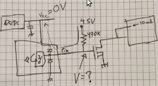
  • What is the architecture of the GPIO / AN pins of this device? Input protection diodes, pull-up/down, output open drain, push-pull, etc
  • What is the state of the all pins during the power-up? For example pin4 of QFN48 package is a digital or an analog input?
  • Can I configure any digital pin as MISO, MOSI, SCLK or CS?

thanks in advance,
gaston

Parents Reply
  • Yes, with low-power MCU it's a common issue - if some pin is externally powered even through high resistance, it will feed and accumulate charge on VDD until it reaches a startup threshold, then MCU will try to start, quickly discharging capacitors - and so on.

    I would not even say that this design is safe - when MCU is sleeping, its power consumption can be lower than 1uA, and 9uA passing through the pin can raise the voltage on VDD up to ~4V if there are no limiting components.

Children
  • Okay, everything that occurs to me is to do an experimental test.

    I just made a check connecting the pin P0.07 of an NRF51822 to 3V (assuming it has the same pinmux architecture as the NRF52810) and unpowering the rest of the system. The result is that a voltage of 2.38V appears on VDD that finally powering the uC.

    If I power the P0.07 through a 470k pull-up resistance the generated voltage falls to 500mV. This is not enough to start the uC but it is still undesirable.

    Even though the uC pins are disconnected during the power-Up, I don't feel confident about the hardware configuration that I had suggested. I will have to think about a safer alternative.

    For me we can close this case. Thank you Ketiljo and Dmitry for your help!

    regards,
    gaston

Related