Hello,
my question concerns the layout of a bluetooth antenna & tuning circuitry for an nRF52832. Specifically, about two separate concerns:
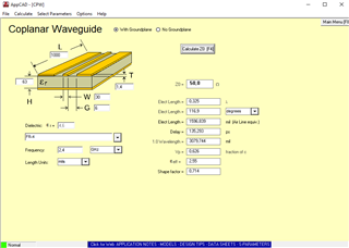
1) Due to the shape of the PCB, the antenna is intended to be placed on an extruding part of the board, sort of like a thin arm. The nRF itself doesn't fit there, so the trace from the nRF to the antenna would probably be slightly longer (up to around 15-20mm). My question is, how long can those traces be until the signal quality starts to noticeably degrade? Or is it just a matter of having to compensate for the longer trace in my tuning circuit?
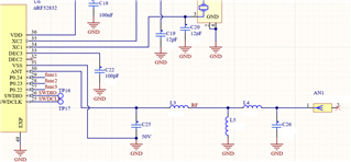
2) The second question is sort of related to the first: should the tuning circuit be placed as close as possibly to the nRF or the antenna? Can/should I increase the distance between individual components on the way to the antenna, or keep the tuning circuit together as close as possible? See below for a schematic of my tuning circuit.
I checked the manual of the nRF52832, and under '53.8 PCB layout example' stands "For all available reference layouts, see Reference layout nRF52 Series." with a link to the Reference layout but the link only leads to a "Page not found" error -- so I figured I'd ask my layout related questions here directly.
Greetings


