This post is older than 2 years and might not be relevant anymore
More Info: Consider searching for newer posts

nrf52840 schematic review

Hi,

We are developing the Bluetooth based weight scale product.

We have successfully developed the project using nrf52840 DK board but now we are planning to develop the custom board using same.

I want you to look into whole schematic and let me know if anything need to change.

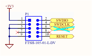
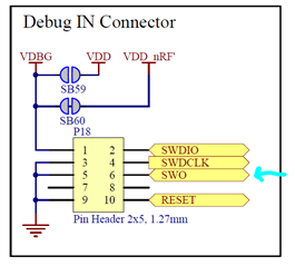
also just to clear my doubt ,check JTAG pin connection(P1 connector - SWD pin) we are planning to use those pins to flash and debug the controller. So need to make sure those connection are perfect.

Thank you in advance.

Rahul Kidecha


0876.nrf52840.rar

Parents
  • Hi Rahul,


    There was only the schematics in the included file, we also do review the PCB layout so feel free to include that as well. 

    If you are using Altium to develop the project we do have reference files available for download here.


    Pin 6 on P1 does not connect to SWDIO. you can leave this pin blank. Pin 6 is used as a debug pin in the DK design and is connected to P1.0(AD22) pin on the SoC.


    Rest looks ok,

    Regards,
    Jonathan


Reply
  • Hi Rahul,


    There was only the schematics in the included file, we also do review the PCB layout so feel free to include that as well. 

    If you are using Altium to develop the project we do have reference files available for download here.


    Pin 6 on P1 does not connect to SWDIO. you can leave this pin blank. Pin 6 is used as a debug pin in the DK design and is connected to P1.0(AD22) pin on the SoC.


    Rest looks ok,

    Regards,
    Jonathan


Children
No Data
Related