This post is older than 2 years and might not be relevant anymore
More Info: Consider searching for newer posts

nRF5340 + nRF21540 connection

Hi,

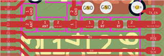
I have questions about the connections between the nRF5340 and the FEM nRF21540.

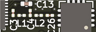
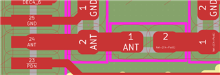
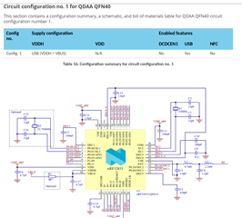
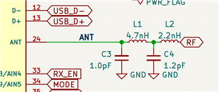
The nRF5340 has these components:

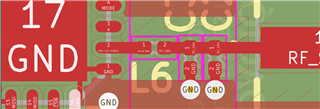
And the nRF21540 has this component:

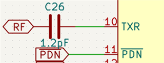
I wonder if C3,C4,L1 and L2 are needed between these two IC.

Wouldn't be enough just used the C26?

I am using a single antenna.

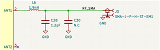
The C28, C30 and L6 are needed to match the antenna impedance of 50Ohms, but I am not sure if it's actually needed to match impedance between ICs.

The same questions goes for the nRF52833 + nRF21540.

Any suggestions?

Thanks and best regards,

Jose Pablo Castro,

  • Hi Jose

    All the components shown on the nRF5233 and nRF21540 schematics are mandatory. Any antenna matching components comes in addition to L6, C28 and C30. 

  • Hi ketijo,

    If I understand you correctly, there's no need to add or remove any component (Capacitance or Inductance).
    Am I right?

    I got another question regard to PCB board.

    I am placing all components as close as possible, including the SMA Connector like this:

    Between nRF52833 and nRF21540:

    3D View (Kicad Nightly)


    And between nRF21540 and SMA Connector:

    3D View:

    The stack-up is this:

    And the width calculation for 50 Ohms is this:

    Is this components placement and distance correct or should I increase the distance between components?

    I am using the exact width of 0.355473 mm except between nRF52833 pin 24 (ANT) and C3 (The actual size is 0.3 mm)


    as far as I understand the width is ok for 50 Ohms but I have my doubts especially if there could be any problem between C3 and pin 24 of nRF53833.

    Any suggestion or recommendation?

    Thanks and Best Regards,

    José P. Castro

  • You can do it like this, no problem. The lines are really too short to give you problems with the impedance. Just place the component as compact as you can and you'll fine.

    cheers,

    Ketil

  • HI Ketil,

    I got another question.

    If I understand it right the power supply configuration for High voltage mode with USB(VDDH=VBUS) in circuit configuration no. 4:

    and the datasheet says:

    so, with this configuration VDD is a power source itself.

    Can the nRF21540 VDD be connected to nRF5340 VDD in this configuration?

    Same question for nRF82833 with configuration 1 for QDAA QFN40

    And another question.

    In a 4 layer stack-up, if I used one inner layer for power signals:

    Is there any problem having VDD below the IC (both nRF52833 and nRF5340), or should I keep that area as GND?

    The idea is to have signals only on the outer layers and GND and Powers in inner layers.

    Thanks and Best Regards,

    Jose Pablo Castro,

  • The regulator in the nRF53 can't supply the nRf21540 with enough current so you will need a separate regulator for the FEM in this case Also, the nRF82833 isn't designed to supply anything from the VDD net.

    It's preferred to have ground plane as the next layer under the radio.

Related