This post is older than 2 years and might not be relevant anymore
More Info: Consider searching for newer posts

nRF52832 custom board; RF antenna design and tuning

Hello, I am brand new to antenna design and especially antenna tuning and want to know if my antenna tuning design/method would work. 

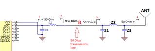
First I will be tuning with a VMA (nanoVGA-F V2) where I will connect from the SMA on the VMA to a u.FL connection (J1) on my board. You can see this in the schematic below.

I am using the Rainsun AN9520-245 antenna (LINK) as well.

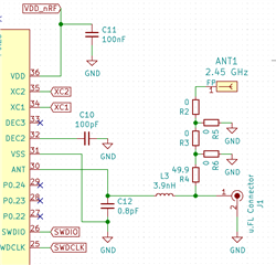
After the capacitor (C12) and inductor (L3)  (I believe these should always be used??), I added the u.FL connector to hook up to the VMA and then I have added a 49.9 Ohm resistor to match the antenna impedance of 50 Ohm while also leaving some resistance for the traces.

All of the 0 Ohm resistors are SMD_0603. I plan to take these off and add applicable capacitors and inductors in their place while tuning. I also did this layout for the resistors so that it covers both T and Pi tuning layouts that could possibly happen.

I will get these test capacitors and inductors from these two links LINK and LINK. I feel like these small values will be good for tuning purposes but the most important thing is that they are SMD_0603 so they will fit in place of the 0 Ohms resistors.

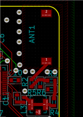
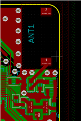
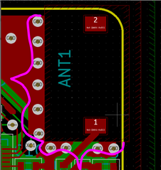
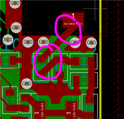
The layout of the board is above. I read a lot of different things about how to go about this and I tried to stick to those design concepts like not having anything under the antenna, ground vias around the "keep out zone", keep chip-to-antenna trace as short as possible, etc. Is there anything else that I may not be doing correctly layout-wise?

Is this a good way to go about tunning my antenna and are there any issues with my layout/design?

Any help is greatly appreciated!

  • Hi,


    Will try to guide you as best i can on this, but i also want to inform you that we at Nordic do provide tuning services for both the antenna radio as well as schematic and HW reviews.

    Here is some links to some guides we have on HW design.
    (+) General PCB design guidelines for nRF52 series - Hardware design, test and measurement - nRF5 SDK guides - Nordic DevZone (nordicsemi.com)
    (+) nRF52832 Specific PCB Guidelines - Hardware design, test and measurement - nRF5 SDK guides - Nordic DevZone (nordicsemi.com)

    And for the nrf52832 there is a Errata 138 that adresses some radio issues. Grounding or decoupling pin 37 and 38.

    Here is the PCB guidelines and layout for the nrf52832, i guess that you might have looked at this all ready. 


    Firstly the there are two main parts in this system, the radio and its matching network and the antenna and its matching network.


    For the first part, the radio we strongly recommend that you not only follow the recommendation from the schematic, but also the reference layout. 

    and it looks like you have followed our recommendation to some degree. Reason for why we say that you should follow the layout is due to the fact that there is stray capacitance and inductance that will change how it well it preforms, so with the component values we have recommended the layout should also match. When the deviation in the layout is to great then we can not guarantee that the radio will preform optimally. 


    The specific layout helps match the output to 50 ohms and filter the harmonics. Filtering the harmonics is equally as important.


    I will get these test capacitors and inductors from these two links LINK and LINK.

     Great choice of components. 


    I am using the Rainsun AN9520-245 antenna (LINK) as well.

     The antenna looks ok, but in your layout you are covering 2 sides of the antenna, and maybe more with a casing\cover?

    My concern is that when looking in the data sheet of the antenna it looks like they have quite the huge clearance on 3 sides of the antenna.

    Do you have enough space on all sides for the antenna to operate as recommended?

    As for matching for the antenna i think a pi-network is ok.


    As for the layout, you have the right thoughts but i is not ideal. The transmission line is prone to stray capacitance so keeping it 50 Ohms might not be the case here. I like to recommend that you use a grounded coplanar waveguide as the transmission line. 


    The signal source should try to enter in a straight line and not at an angle. The two sections is to close to one another and could interfare with it self and is probably not 50 Ohms in impedance. 


    Regards,
    Jonathan

Related