Hello,
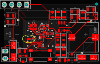
I have been using the nRF52840 DK board and have designed a PCB based on it. I made a previous post asking some questions before designing the PCB, so this is a follow-up.
https://devzone.nordicsemi.com/f/nordic-q-a/78124/going-from-nrf52840-dk-to-pcb
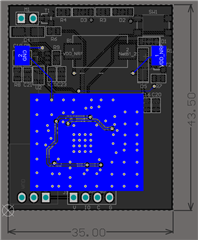
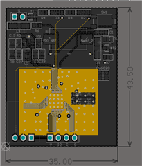
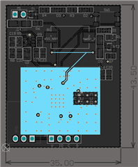
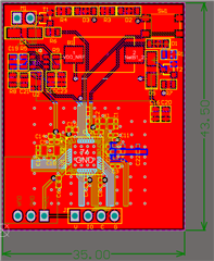
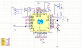
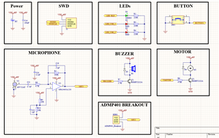
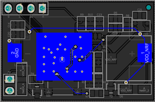
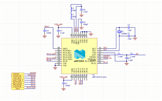
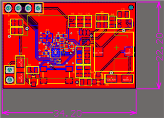
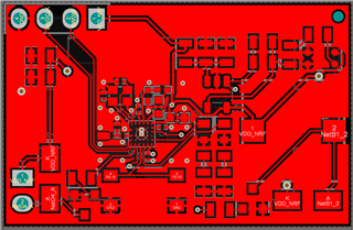
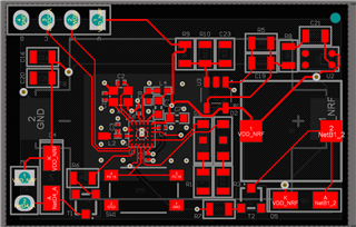
With the schematic, I haven't changed anything except adding my connections to the pins, and using Generic No ERC markers on the unused pins. The PCB I kept the same and add my components above it, and the battery on the bottom layer. The only changes I made were extending the top layer ground polygon (red), and using the vias around the nRF chip to branch out a ground and VCC line.
1) Is my PCB fine to manufacture or are there any changes I should make to it. My design uses a few GPIO pins, analog pins, and Bluetooth to communicate with. I used configuration 6, from the reference design.
2) On the schematic there is an optional section with a crystal connected to XL1/XL2. Do I need to have this on my design?
Kind regards,
J