This post is older than 2 years and might not be relevant anymore
More Info: Consider searching for newer posts

Different ways to place RF matching/filter components in PCB

Hi.

Below is used the same schematic for nRF52805 but with different placement for RF components.

What are the pros and cons of each one? Is there one that is "better" or most recommended? 

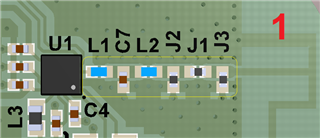
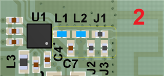
2 - shorter RF path but with 'stubs'. This method is shown in the reference layout of nRF52805.

1 - longer RF path but without 'stubs'. In a previous desing of layout of a beacon, the Nordic's engineer recommended this method instead of method "1".

Regards.

  • Hello,


    Adding stubs to a RF line will add extra capacitance and inductance to the line. For example will a open stub shorter than one quarter wavelength act as a shunt capacitance while a shorted stub as a shunt inductor. This means that the same component values of the matching networks in method 1 and 2 will yield different results. Short stubs like in method 2 will generally not introduce problems at these frequencies, when the length of the stub is close to the quarter wavelength of the signal it will act as a resonant circuit.

    What are the pros and cons of each one?

    Method 1 adds no stubs in the line that can introduce unwanted capacitive or inductive reactance, while it uses more space on the board.

    Method 2 is more compact, but the values for the radio matching network in the reference design may not yield the results that's intended.


    Is there one that is "better" or most recommended? 

     The best method is to stick as close as possible to the reference design. But both method will work, given that the radio matching network is tuned to give the best output power while keeping the harmonic emission below the regulatory limits.


    Best regards,

    Bendik Heiskel

Related