This post is older than 2 years and might not be relevant anymore
More Info: Consider searching for newer posts

Needs to verify Power Supply for nRF52840

Hi,

I would to design a custom PCB with nRF52840 SOC.

I have two different power source:

1. 3V Lithium coin cell

2. 3.7V LiPO battery with charging circuitry

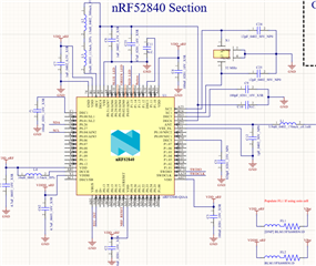
I will use one of the power source for nRF52840. So I would like to confirm about the attached schematic.
Correct me if I am doing anything wrong.

Thanks.

Parents
  • Hi,

    Is your intention to use the nRF in Normal voltage mode if you're using the coin cell by populating FL1 resulting in VBAT, VDD_nRF and VDDH_nRF being shorted together?

    Overall what's important is the supply follows the requirement as described in the PS, namely in that it's stable and respects the minimum VDD rise time. Some other comments regarding your design:

    • The USB signal pins D+ and D- can not be used as normal GPIO pins. You should therefore move RTC_INT from D-
    • Can you confirm that C2 is 100 nF?
    • The antenna path should be as in the reference design. I can't tell if it is as the screenshot is cut a bit short.

    regards

    Jared 

Reply
  • Hi,

    Is your intention to use the nRF in Normal voltage mode if you're using the coin cell by populating FL1 resulting in VBAT, VDD_nRF and VDDH_nRF being shorted together?

    Overall what's important is the supply follows the requirement as described in the PS, namely in that it's stable and respects the minimum VDD rise time. Some other comments regarding your design:

    • The USB signal pins D+ and D- can not be used as normal GPIO pins. You should therefore move RTC_INT from D-
    • Can you confirm that C2 is 100 nF?
    • The antenna path should be as in the reference design. I can't tell if it is as the screenshot is cut a bit short.

    regards

    Jared 

Children
Related