Hello,
After reading many things, I would like someone to confirm or correct my understanding. I believe this will be great clarity for others as well.
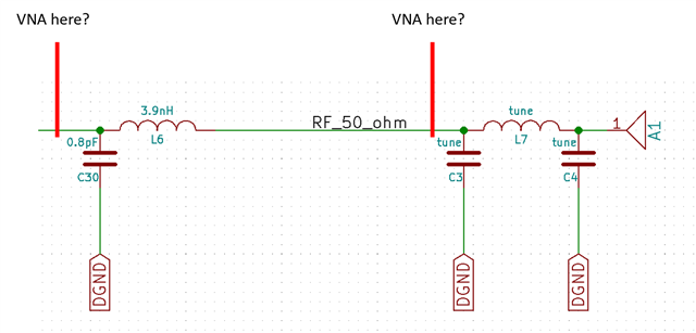
The nrf52 requires matching components right after the antenna pin (a capacitor and inductor).
Q1) Should this be 0.8 pF and 3.9 nH or 1.0 pF and 3.3 nH?
After this, a 50 ohm rf trace with a correctly computed width follows up to my chip antenna.
Q2) At the end of this trace and just before the antenna, should be a pi matching circuit?
Finally, I need to evaluate this design with a VNA for impedance matching.
Q3) Where exactly do I measure with the VNA? Just after the nrf52 pin but before the nrf52 capacitor and inductor matching components? Or just after the rf trace but before the pi matching? Or both?
The PCB and traces are quite small and I don't see how I could possibly measure this.
Q4) Should I make another PCB just for measuring this consisting just of everything coming out of the antenna pin on the nrf52? Or just everything from pi matching and antenna.
Check my diagram to better understand my questions. Thank you!
Any clear answers and pictures would be greatly appreciated.