This discussion has been locked.
You can no longer post new replies to this discussion. If you have a question you can start a new discussion

excessive capacitance on GPS and LTE pads

Hi everyone,

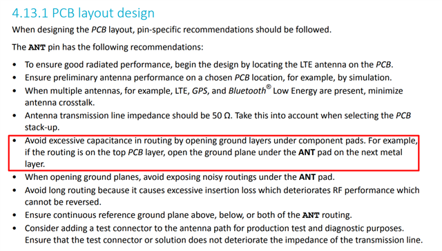
I'm designing with nRF9160, and I found nordic's suggestion on the PCB layer, which is underneath the GPS and LTE pad should be removed. I'm curious if the impedance will be affected negatively by doing so. Does anyone have experience with this?

Thanks!

Ye-Sheng
Parents
  • Hi,

    I'm not sure what you mean by removing this suggestion. Do you not have a groundplane under the routing plane in your design? Either way, you'l have to tune specifically for your PCB, any big changes like removing a layer will affect the impedance.

    regards

    Jared 

  • Hi Jared,

    Sorry for my wording. I was asking if removing the ground plane under the pads (as the guideline says) will have a negative impact on impedance.
    I'm thinking of following it, but a colleague has a different opinion on it. (saying it may be worse in terms of impedance mismatch)

    Thanks,

  • Hi,

    I think that it will change the impedance. But I don't think it should matter in the long run, as you either way would have to tune the board when you're done. If you want to do a HW review of your RF design when you are done, then you can create a new private case and attach the schematic and Gerber files. One of our RF engineers will the review your design and suggest improvements if needed. Also note that the Hardware integration guide shows how the PCB design should be. 

    regards

    Jared 

Reply
  • Hi,

    I think that it will change the impedance. But I don't think it should matter in the long run, as you either way would have to tune the board when you're done. If you want to do a HW review of your RF design when you are done, then you can create a new private case and attach the schematic and Gerber files. One of our RF engineers will the review your design and suggest improvements if needed. Also note that the Hardware integration guide shows how the PCB design should be. 

    regards

    Jared 

Children
Related