failure in spurious emission test in RX mode with design based on pre-certified module

Hi,

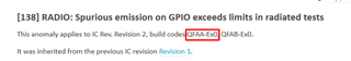
In our design we use Fanstel BM832 module, based on nRF52832 chip. We have failed spurious emission in ETSI RX mode. Rx LO at ~4958 MHz exceeds the limit by 0.3 dB. I know that it is known issue, described in errata (point 138). I contacted with Fanstel with this issue, but they claim that the module is below the limit.

In our design, we do not use P.025 and P.026 pins, they are only connected to test points with very short (<3 mm) traces and one via per pin.

Nordic's chip in our module which failed the tests is marked N52832 / QFAAE1 / 1934IN. Chip inside Fanstel's module, which have been subjected to Fanstel's test is probably marked as N52832 / QFAAE0 but I am not sure.

I assume that errata 138 concerns to both chips described above - am I right?

My question are:

1. is it possible to pass the regulatory test without addition of 12 pF caps on P.025 and P.026 or tying pins to  GND? On Fanstel's module there are no 12p caps, nor the pins are tied to GND.

2. did you face the problem, that module manufacturer got an certification, but end product containing the module failed the certification?

3. Is it possible that Fanstel used older chip with different hardware version code in which the problem did not occur?

Best regards

Parents
  • Hi Ketil

    Thank you for theanswer. I have one more question, because we simply do not have enough time to change layout before launching device to market - what do you think about configuration of P0.25 and P0.26 as push-pull output and driving it low? May it solve the problem?

    Best regards,

    Jakub Kwolek

  • Unfortunately, this won't work. The VCO that's generating the LO (local oscillator for the receiver) is internally grounded near pin P0.25. The VCO runs at 2*LO and the ground wire is carrying this signal. The signal is coupled to the nearby bonding wire and radiates from the track that runs from this pin. If you ground the pad by driving it low, you will only do this on the inside of the bonding wire. While the impedance will change when doing this, the 2*LO signal will still couple through to the next bonding wire. Hence you have to decouple this signal on the outside of the chip. 

Reply
  • Unfortunately, this won't work. The VCO that's generating the LO (local oscillator for the receiver) is internally grounded near pin P0.25. The VCO runs at 2*LO and the ground wire is carrying this signal. The signal is coupled to the nearby bonding wire and radiates from the track that runs from this pin. If you ground the pad by driving it low, you will only do this on the inside of the bonding wire. While the impedance will change when doing this, the 2*LO signal will still couple through to the next bonding wire. Hence you have to decouple this signal on the outside of the chip. 

Children
No Data
Related