Custom NRF52810 board not advertising and hanging on nrf_sdh_enable_request()

Hello all,

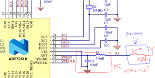
I have recently developed a custom board that uses an nrf52810. It also contains an accelerometer as well as some hardware for regulating the voltage and charging a battery. The issue I am having is that the device is unable to advertise. I have been searching around the internet for days however have been unable to find a solution to my problem. I am using sdk17.1.0 and softdevice s112 v7.2.0. I have been trying to use the ble_blinky_pca10040e example to help me start learning to develop for this board. My board does not contain a LF clock and therefore I set it to use the RC in the sdk_config. I have also set the ram and flash sizes appropriately. I have made numerous other modifications to the sdk_config however nothing appears to work. I at first used rtt viewer to see the logs from the device while it ran and it would sometimes throw errors while attempting to set BLE_CONN_CFG_GAP, BLE_GAP_CFG_ROLE_COUNT, etc, sometimes with a fatal error thrown as well. I started using SES to debug the application. When the program is loaded onto the device it runs until it hits ble_stack_init and then either halts on the register at 00000A60, or (more often) gets stuck on the line SVCALL(SD_SOFTDEVICE_ENABLE, uint32_t, sd_softdevice_enable(nrf_clock_lf_cfg_t const * p_clock_lf_cfg, nrf_fault_handler_t fault_handler));. The errors commented above the call make me think that it has something to do with the LF clock config however if I check the configuration it is correct. (set to RC, accuracy to 1, RC_CTIV 16, RC_TEMP_CTIV to 2), and I can also see the correct values in the variable when debugging. The device is able to run examples that do not involve BLE (like the blinky example) without issue. This is my first time taking on a project this large and I will admit at this point I am feeling rather lost. Any assistance is greatly appreciated. I am also happy to upload any code or hardware files should anyone require them. 

Thank you!

  • Hi there,

    The ram and flash sizes shouldn't be adjusted if you're using a PCA10040e example. If you're using a custom board then you need to add a custom board file for the pins on the board to be mapped correctly. Can you try flashing the attached example to your board? It writes directly to the registers of the nRF and starts transmitting with the radio. This example is not dependent on the board file so you don't need to add one for this to work. If the resources that is needed to use the radio has been configured correctly, then you should see some radio activity if you use the nRF Connect RSSI app.

    1. Just copy and past the code into the blinky PCA10040e example.
    2. Build the project and flash it to your IC.
    3. Open the RSSI app on your computer with a devkit.
    4. See if you see any radio activity.

    Could you also upload your schematics(I made the case private)?

    #include <nrf.h>
    
    int main(void)
    {
      // Packet to send
      uint8_t packet[16] = "demopacket";
      
      // Start HFCLK from crystal oscillator. The radio needs crystal to function correctly.
      NRF_CLOCK->TASKS_HFCLKSTART = 1;
      while (NRF_CLOCK->EVENTS_HFCLKSTARTED == 0);
      
      // Configure radio with 2Mbit Nordic proprietary mode
      NRF_RADIO->MODE = RADIO_MODE_MODE_Nrf_2Mbit << RADIO_MODE_MODE_Pos;
      
      // Configure packet with no S0,S1 or Length fields and 8-bit preamble.
      NRF_RADIO->PCNF0 = (0 << RADIO_PCNF0_LFLEN_Pos) |
                         (0 << RADIO_PCNF0_S0LEN_Pos) |
                         (0 << RADIO_PCNF0_S1LEN_Pos) | 
                         (RADIO_PCNF0_S1INCL_Automatic << RADIO_PCNF0_S1INCL_Pos) |
                         (RADIO_PCNF0_PLEN_8bit << RADIO_PCNF0_PLEN_Pos);
      
      // Configure static payload length of 16 bytes. 3 bytes address, little endian with whitening enabled.
      NRF_RADIO->PCNF1 =  (16 << RADIO_PCNF1_MAXLEN_Pos) |
                          (16 << RADIO_PCNF1_STATLEN_Pos) |
                          (2  << RADIO_PCNF1_BALEN_Pos) | 
                          (RADIO_PCNF1_ENDIAN_Little << RADIO_PCNF1_ENDIAN_Pos) |
                          (RADIO_PCNF1_WHITEEN_Enabled << RADIO_PCNF1_WHITEEN_Pos);
      
      // initialize whitening value
      NRF_RADIO->DATAWHITEIV = 0x55;
      
      // Configure address Prefix0 + Base0
      NRF_RADIO->BASE0   = 0x0000BABE;
      NRF_RADIO->PREFIX0 = 0x41 << RADIO_PREFIX0_AP0_Pos;
      
      // Use logical address 0 (BASE0 + PREFIX0 byte 0)
      NRF_RADIO->TXADDRESS = 0 << RADIO_TXADDRESS_TXADDRESS_Pos;
      
      // Initialize CRC (two bytes)
      NRF_RADIO->CRCCNF = (RADIO_CRCCNF_LEN_Two << RADIO_CRCCNF_LEN_Pos) |
                          (RADIO_CRCCNF_SKIPADDR_Skip << RADIO_CRCCNF_SKIPADDR_Pos);
      NRF_RADIO->CRCPOLY = 0x0000AAAA;
      NRF_RADIO->CRCINIT = 0x12345678;
      
      // Enable fast rampup, new in nRF52
      NRF_RADIO->MODECNF0 = (RADIO_MODECNF0_DTX_B0 << RADIO_MODECNF0_DTX_Pos) |
                            (RADIO_MODECNF0_RU_Fast << RADIO_MODECNF0_RU_Pos);
                            
      // 0dBm output power, sending packets at 2400MHz
      NRF_RADIO->TXPOWER = RADIO_TXPOWER_TXPOWER_0dBm << RADIO_TXPOWER_TXPOWER_Pos;
      NRF_RADIO->FREQUENCY = 0 << RADIO_FREQUENCY_FREQUENCY_Pos;
      
      // Configure address of the packet and logic address to use
      NRF_RADIO->PACKETPTR = (uint32_t)&packet[0];
      
      // Configure shortcuts to start as soon as READY event is received, and disable radio as soon as packet is sent.
      NRF_RADIO->SHORTS = (RADIO_SHORTS_READY_START_Enabled << RADIO_SHORTS_READY_START_Pos) |
                          (RADIO_SHORTS_END_DISABLE_Enabled << RADIO_SHORTS_END_DISABLE_Pos);
      
      // Continuously send the same packet
      while (1)
      {
        NRF_RADIO->TASKS_TXEN = 1;
        while (NRF_RADIO->EVENTS_DISABLED == 0);
        NRF_RADIO->EVENTS_DISABLED = 0;
      }
    }
    

    regards

    Jared 

  • Hello Jared,

    Thank you for your response, I am going to attempt to run the code you have provided right now. I am also uploading a file containing the schematic and board files, as well as screenshots of both for you. I do not currently have a dev kit on hand however I actually have an nrf52832 variant coming in the mail tomorrow for a reference design. For now I will use the rssi scanner in the nordic IOS app. nrf52810 Board Files.zip

  • Hey Jared,

    So I ran the code that you provided me however it does not appear as though it is sending a signal, although I won't know for sure until I am able to test it with the dev kit tomorrow. I also debugged the code after I ran it and it also appears to hang on the same register that the ble_blinky app does. A part of me is starting to think that it may be the HF clock is not functioning properly, however the layout and connections appear to be fine to me. This is the HF clock I used on the device: www.lcsc.com/.../SMD-Crystal-Resonators_Yangxing-Tech-X201632MKD4SI_C108165.html

  • Hi,

    Looking at your design I see several points that should be addressed:

    1. DEC4 is not connected to anything
    2. What is the circuit on P0.25 and P0.28 doing? 
    3. The antenna path does not follow the reference design. The antenna path should consist of two parts. The first part is the matching network for the radio which should be a 0.8 pF parallel capacitor and a 3.9 nH series inductor as shown in the reference design below. In addition to this you'll need a matching network for your antenna. I checked the datasheet of the chip antenna that you're using and it specifies a parallel capacitor and a series inductor seen from the antenna. This should be added in series to the matching network of the radio.

    The application shouldn't assert even though you haven't added the matching network. That is probably related to my DEC 4 comment above. But you have a good signal without a matching network for the antenna. You also have to do a antenna tuning at some point.

    Looking at your PCB design, It seems the GND layer is missing?

    regards

    Jared 

  • Hey Jared,

    Sorry, I forget to mention that I reworked the designs slightly and connected dec4 correctly, before I did that the devices would not even power up. It was a mistake I made because easyeda had incorrect pin labels and I did not check (woops). The circuit on p0.25 and p0.28 was the dc/dc regulator set up that I fixed. In my next design I will make sure to correct the antenna issue, thanks for pointing that out. That said the chip still hangs on the SVC call for enabling the ble stack. Do you know if any examples exist that are programmed specifically for the nrf52810? I have a dev kit coming in soon as well and will be able to use that as a reference. Also the pcb is just 2 layers so there is a copper layer on the top layer that the ground nets to.

    Thanks again Jared!

Related