
Hi,
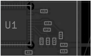
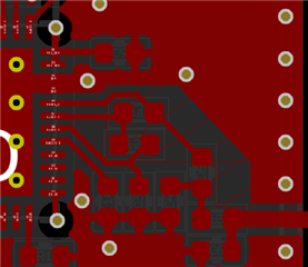
I am new to microwave board design, so I'd like a little advice please. I have attached photos of the 2.4ghz section of my board and would like to know if the component layout is okay. The circuit should be identical (with reference to DC resistance) to the reference design, but I just need to know if it's okay to rearrange the component locations/orientations as I've done.
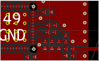
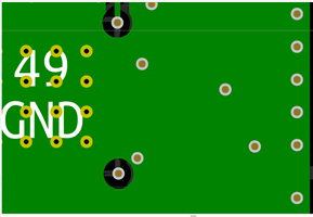
I noticed in the reference design there are not ground planes near the RF section. I presume that's to reduce the stray capacitance and thereby keeping the impedance more constant.
Should I add keepout zones?
Thanks in advance!

