Potential risks if voltage is applied to a GPIO pin when the chip is not powered (VDD = 0.0V)

Hello,

The company I work for uses an nRF52840 PCBA for one of its project. During production, the board will be placed under test using a custom-built fixture. Due to the nature of our setup and testing procedure, there was found to be a step where a positive voltage (~2V) could be present on a GPIO pin when the rest of the board had no power (VDD = 0V). Our electrical engineers are currently brainstorming methods of altering the fixture hardware to accommodate this, as they believe it can damage the chip. Though I trust their knowledge, I could not find further explanations or warnings on this in the product specification. Is anyone able to provide more information regarding this?

Thanks

Parents
  • Brief answer is it depends on what is attached to the other nRF5240 pins. With no VCC the tester driving voltage into an i/o pin powers up the entire nRF52840 since the internal schottky clamp diode to the internal VCC - designed to protect the i/o pin against latchup - is forward biased and connects the tester pin voltage to internal VCC. In a quiescent state let's say that takes 5mA; the pin will probably survive. Users do this all the time - not intentionally - by leaving an FTDI USB serial port connected to the nRF52840 when turning off power.

    If the nRF52840 was not already powered when the tester applied the voltage to the pin, damage is more likely; this is because of what is connected to other pins, and the worst case is that fat 10uF or 47uF capacitor on VCC which has to be charged to the observed 2 volts through the tiny scottky protection diode which is lifting internal VCC. This can be alleviated by programming the expensive automated tester to limit the current output on the test pin to something reasonable (say 200uA); if it's a home-brew simple tester that's not an option of course although a resistor may work.

    There are other issues; even if the diode doesn't fail, the ability to power-on reset by removing and re-applying power is lost since the tester holds the internal VCC above the reset or brown-out voltage, leading to strange behaviour. Using a series resistor doesn't help here, since as the voltage is lowered but still above reset the current required to hold up is only a few nA

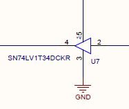
    The fix? Add a level shifter to the tester to any pin which can drive voltage to the nRF52840 when no power is applied to the latter. Power the level shifter from the nRF52840 VCC directly (not the supply to an external regulator, direct to the nRF52840 VCC).

    Be aware other side effects can occur; if the tester has a very high slew rate on the output pins any inductive connection (12" test wire) can deliver a sufficiently high kickback voltage to the pin to break down the schottky despite the typical human-body ESD protection rating. Fix that by programming a "reasonable" slew rate to the tester pin, say a few 100 nSecs. Simple testers don't have this issue as the slew rate is already limited. 5pSecs at 5mA and 1uL is 1,000 volts kickback; ok 5pSecs is pretty fast but still a risk.

    Lastly the 2 volts is typical of driving a current-limited tester output pin (maybe a MSP430) into an unpowered nRF52 i/o pin assuming the tester pin start limiting current.

  • Thanks for the explanation! It helps to understand the mechanism of action as you explained, as the product spec doesn't seem to cover this outside of the maximum ratings section, which states that the level of a GPIO pin shouldn't exceed VDD + 0.3V

Reply Children
No Data
Related