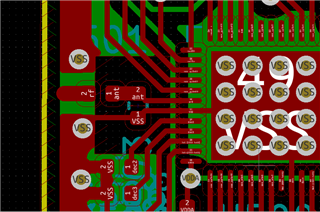
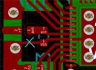
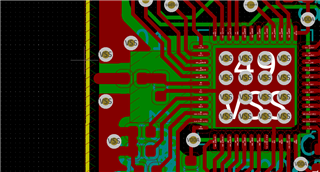
NRF52832 PCB Layout Review

Hello,

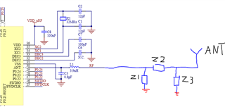
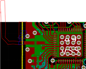
I'm wrapping up the layout of a board based on the NRF52832 (DCDC). I've tried to replicate the reference design as close as possible. I'm using Kicad and had to import the Eagle design, and wasn't sure on the fill/keep out areas close to the antenna which appears to be lost in the import process. I'm not a RF engineer and would appreciate some feedback if the layout of this portion looks acceptable, or if any changes are recommended.

Also we are planning to pot the electronics in epoxy into something about the size of a fist. The antenna will be sitting at the edge of this material. Will this require changing the RF tuning elements to get good performance? The product needs to achieve 75+ feet of communication. Thanks so much for the help! I can provide more information if that would be helpful.

Parents Reply Children
  • Hi,

    Just want to clarify somethings regarding the antenna and ref designs. 
    - there is not antenna in the circuit reference design only a radio matching network. 
    - we do have antenna reference in our DK hardware files.

    So if you where to follow only the circuit reference design then you would not have an antenna, so you need to include an antenna in the design or else you will not be successful wit radio communication. 

    You can gett the HW files for the DK here:https://www.nordicsemi.com/Products/Development-hardware/nRF52-DK/Download?lang=en#infotabs 


    "A matching network is needed between the RF pin ANT and the antenna, to match the antenna impedance (normally 50 ohm) to the optimum RF load impedance for the chip." and  " All the reference circuits are designed for use with a 50 ohm single end antenna."

    So that means that you should make sure that it is matched on both the chip side and the antenna side. 


    Here is a rough illustration of what a schematic could look like. So here we have the C3 and L1 as the matching and filtering components for the radio pin, and then we have the transmission line that leads to the the antenna matching components. We often do recommend a full pi network but it is not always needed, as you can see in our DK design we use a PCB trace antenna only have a singel shunt capacitor so that would be Z3 in the illustration above. 


    So to be able to use the PCB that you have shared here with me for any type of radio communication then you need to add a antenna, i did a rough sketch to illustrate what that could look like. 


    Marshal said:
    How crucial is antenna size and shape?

    It has major impact on the performance. 


    Marshal said:
    Lastly is the tuning process changing L's and C's, or would it require a whole new board spin?

    There will be two tuning processes, one would be for the radio, to ensure that it provides enough power and that it filters the harmonics sufficiently. Then there is the tuning of the antenna, to make sure that it is 50 Ohm and a low enough VSWR.  We at Nordic can provide this services.

    Regards,
    Jonathan

Related