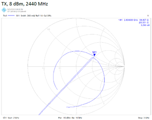
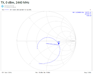
I am tying to match the nRF52840 rf output to my 50 ohm 2.45GHz pcb antenna. What is the optimum rf impedance for best transmitter/receiver performance? The markings on the chip are N52840 QIAAC0 1908GK.
Thankyou,
Doug
I am tying to match the nRF52840 rf output to my 50 ohm 2.45GHz pcb antenna. What is the optimum rf impedance for best transmitter/receiver performance? The markings on the chip are N52840 QIAAC0 1908GK.
Thankyou,
Doug
Hello Doug,
I notice that you set the status of this case to "Open", do you need any more assistance?
I can copy some information from a previous case that asked about the output impedance of the ANT pin of the nRF52833 which has an identical radio to the nRF52840, but has a four component radio matching network instead of three:


The load impedance, seen into the matching network, should be close to 35 - j35 ohm. The impedance seen into the ANT pin doesn't change too much from 8 dBm to 0 dBm mode. This is the impedance measured into the matching network from the antenna side:


If you want to design a matching network optimal for max 0 dBm output power, you can get away with just a shunt capacitor and a series inductor. Provided you ground the shunt capacitor like in the reference layout. A 0.8 pF capacitor and 3.9 nH inductor is a good starting point. Measure the impedance seen into the matching network with the radio in TX mode and adjust for 50 ohm. (Note: Usually when measuring into the matching network, towards the radio, when the radio is in TX mode you would see an impedance closer to ~70 ohm because this gives the best operating conditions (less harmonics) from the PA.)
The additional components are needed to filter harmonics in 4 and 8 dBm mode.
The reason for the extra inductor in the nRF52833 matching network is to have more margins for the harmonics to the radio regulatory limits in 8 dBm mode.
Both the -833 and -840 matching networks are ok in 8 dBm mode, it's just that we wanted to attenuate the harmonics a bit more. If you only use 0 and 4 dBm, you can use the -840 matching network on both devices.
Best regards, Martin S.
Hello Doug,
I notice that you set the status of this case to "Open", do you need any more assistance?
I can copy some information from a previous case that asked about the output impedance of the ANT pin of the nRF52833 which has an identical radio to the nRF52840, but has a four component radio matching network instead of three:


The load impedance, seen into the matching network, should be close to 35 - j35 ohm. The impedance seen into the ANT pin doesn't change too much from 8 dBm to 0 dBm mode. This is the impedance measured into the matching network from the antenna side:


If you want to design a matching network optimal for max 0 dBm output power, you can get away with just a shunt capacitor and a series inductor. Provided you ground the shunt capacitor like in the reference layout. A 0.8 pF capacitor and 3.9 nH inductor is a good starting point. Measure the impedance seen into the matching network with the radio in TX mode and adjust for 50 ohm. (Note: Usually when measuring into the matching network, towards the radio, when the radio is in TX mode you would see an impedance closer to ~70 ohm because this gives the best operating conditions (less harmonics) from the PA.)
The additional components are needed to filter harmonics in 4 and 8 dBm mode.
The reason for the extra inductor in the nRF52833 matching network is to have more margins for the harmonics to the radio regulatory limits in 8 dBm mode.
Both the -833 and -840 matching networks are ok in 8 dBm mode, it's just that we wanted to attenuate the harmonics a bit more. If you only use 0 and 4 dBm, you can use the -840 matching network on both devices.
Best regards, Martin S.
[I MOVED MY QUESTIONS TO A NEW TICKET]
Hello Martin,
[I MOVED MY QUESTIONS TO A NEW TICKET]
For now, to dispense with the attenuator, I programmed a harmless carrier of only -12 dBm. Hopefully, the output impedance at -12 dBm is still representative of the impedance at +0 dBm.
