
I found that one via on nrf5340dk is different from other vias. It has an extra loop and is connected with the external copper layer. What is the purpose of this design? How is this design drawn in ad?
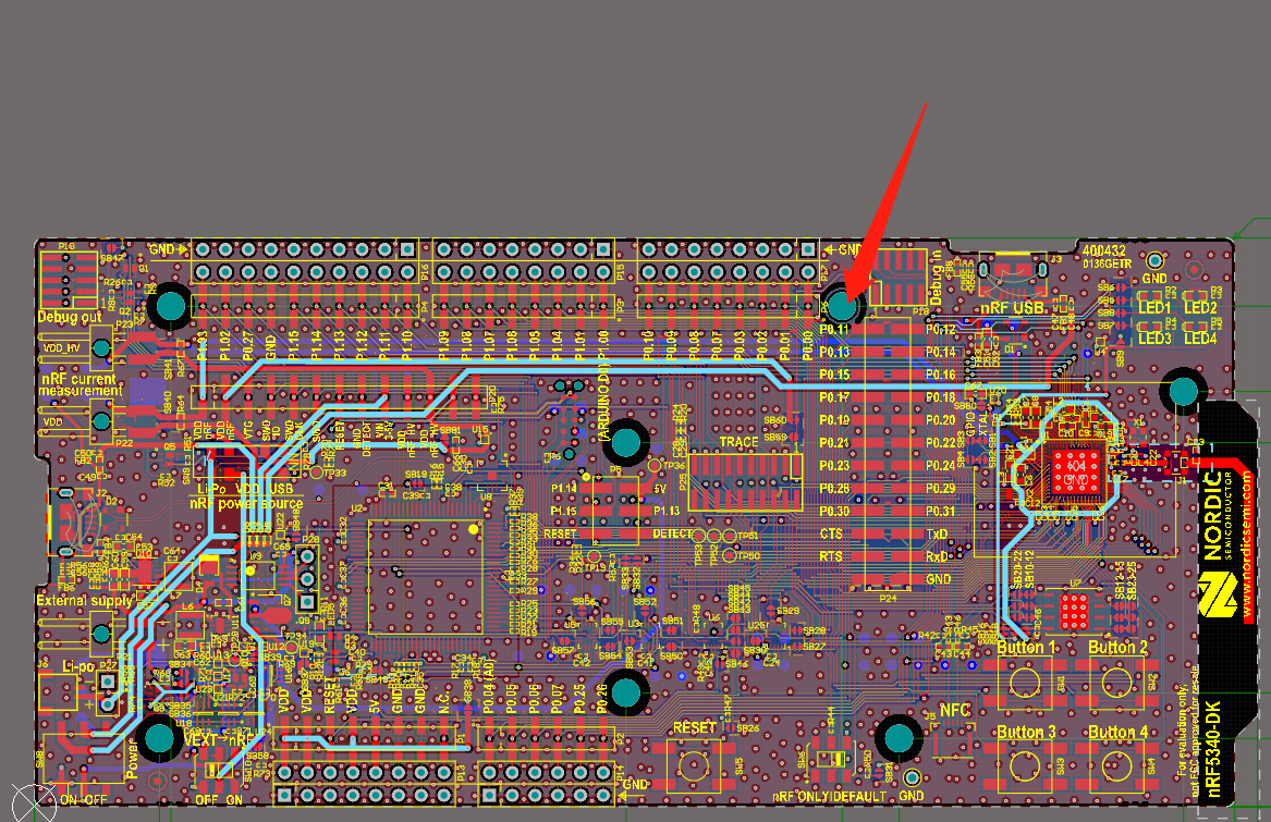
I found that one via on nrf5340dk is different from other vias. It has an extra loop and is connected with the external copper layer. What is the purpose of this design? How is this design drawn in ad?
