Antenna design for 4 Layer 1.0mm PCB

Hi

I am designing a new BLE device and have some questions about the PCB antenna.

The product will be worn on the body.

I have a 4 Layer PCB with 1.0mm with and 35u copper.


TOP        :              RF IC and components, RF trace, antenna, decoupling capacitors, and other signals

Inner 1   :              GND plane

Inner 2   :              VDD plane

BOT        :              GND and some signals


  1. The antenna trace with should have 1.5mm right ?
  2. What should be the distance from the GND planes to the antenna trace ?
  3. should there be a GND plane under the antenna trace ? on what layer ?
  4. should there be a GND plane under the components of the antenna network ?


Layout so far:

TOP

 

Inner 1 (GND plane)

 

Inner 2 (VDD plane)
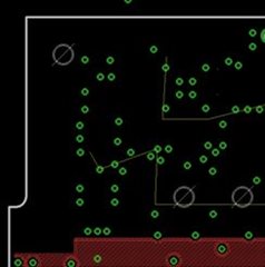
BOT
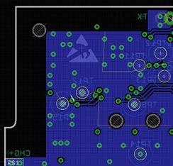
Thanks a lot

M. Aerni

Parents
  • The antenna trace with should have 1.5mm right ?

    A 1.mm wide track for the antenna will work fine.

    What should be the distance from the GND planes to the antenna trace ?

    At least 5 mm, but more than 10 mm is better. 

    should there be a GND plane under the antenna trace ? on what layer ?

    No, that will make the antenna useless. 

    should there be a GND plane under the components of the antenna network ?

    Yes, you will need to have ground under the matching network on the bottom layer (components between the ANT pins and the anetenna)

Reply
  • The antenna trace with should have 1.5mm right ?

    A 1.mm wide track for the antenna will work fine.

    What should be the distance from the GND planes to the antenna trace ?

    At least 5 mm, but more than 10 mm is better. 

    should there be a GND plane under the antenna trace ? on what layer ?

    No, that will make the antenna useless. 

    should there be a GND plane under the components of the antenna network ?

    Yes, you will need to have ground under the matching network on the bottom layer (components between the ANT pins and the anetenna)

Children
Related