This discussion has been locked.
You can no longer post new replies to this discussion. If you have a question you can start a new discussion

PCB Design with nRF52840 SoC

Hi,

First of all thank you for your support and suggestions.

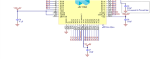
As I am planning to use nRF52840 SoC in my design, (Project: BLE based Environmental sensor). The circuit mainly consist of the sensor (uses SPI), Battery Circuit, Antenna (Mostly U.FL Connector), nRF52840 SoC. Is there any similar PCB design template projects available in order to refer?

Reference Circuit: Nordic Semiconductor Infocenter

Also I have found some points which are not familiar to me, 

  • Power supply: It found from the datasheet that use of DC/DC Regulator has san advantage on Current consumption. (USB is not included in my design) can I go with Circuit configuration no 5 for QIAA aQFN73 (by connecting VBUS to GND) in order to get advantages of DC/DC Regulator?
  • If so, can I design the entire circuit with 3V Battery power supply?
  • Regarding antenna, I would like to do design with U.FL Connector (easy to go with external Antenna), Can I follow the same ANtenna circuit provided in the reference circuit provided in product specification? (or is there any special design required?
  • If I am using only some GPIO pins specially for SPI communication, is it fine to make all other unused pins to float or unconnected?
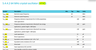
  • How External Crystal oscillator helps my design in terms of power consumption?( I found HFXO helps in reducing current consumption) Is it recommended to use external clocks?
  • There are some capacitors (C10, C13..) which are mentioned as Not Mounted (NC) on the Bill of Material of the reference circuit. What it indicates? Do I need to avoid these capacitors from my design?

I am really interested and looking forward for  valuable suggestions and resposnes. I really do appreciate your help, time and effort.

Thanks and Regards,

Sreejith

Parents
  • Hello Sreejith,

    Thanks for your questions. 

    Power supply: It found from the datasheet that use of DC/DC Regulator has san advantage on Current consumption. (USB is not included in my design) can I go with Circuit configuration no 5 for QIAA aQFN73 (by connecting VBUS to GND) in order to get advantages of DC/DC Regulator?'

    yes you can use the design where VBUS is connected to ground.

    If so, can I design the entire circuit with 3V Battery power supply?

    3V Battery is ok. However you have to careful about the voltage drops. If some sensors consume lot of current for there can be a drop in voltage.

    Regarding antenna, I would like to do design with U.FL Connector (easy to go with external Antenna), Can I follow the same Antenna circuit provided in the reference circuit provided in product specification? (or is there any special design required?

    You can design with UFL connector for external antenna. Then you do not need to design low noise amplifier (LNA). 

    If I am using only some GPIO pins specially for SPI communication, is it fine to make all other unused pins to float or unconnected?

    yes, any unused pin should float or unconnected.

    How External Crystal oscillator helps my design in terms of power consumption?( I found HFXO helps in reducing current consumption) Is it recommended to use external clocks?

    High frequency crystal oscillator is needed in BLE mode (1 Mbps) and in radio transmitting (8 dbm). The 64 MHz crystal oscillator (HFXO) is controlled by a 32 MHz external crystal. It is recommended to use a crystal with lower than maximum load capacitance and/or shunt capacitance. A low load capacitance will reduce both start up time and current consumption. This way external oscillator can help your design.

    There are some capacitors (C10, C13..) which are mentioned as Not Mounted (NC) on the Bill of Material of the reference circuit. What it indicates? Do I need to avoid these capacitors from my design?

    This is from the older version of SOC. you may keep this in design. I will let you inform details on Monday about this. 

    I hope it will help. 

    Have a nice weekend.

    Best Regards,

    Kazi Afroza Sultana

  • Hallo Kazi Afroza Sultana,

    Thank you for your detailed answer and for your valuable time. It really helping me for my first design. Still I am interested to get some more clarrification on your answers,

    1. According to Nordic Reference circuit configurations, Config 5 is with external battery (VDD), DCDC1 and also with USB (VBUS), but Config 6 is with external battery (VDD), No DCDC, No USB. Which configuration would be more suitable if we are interested to reduce power consumption? If config 5 (because of DCDC), can I connect the USB(VBUS) to ground because I am not using USB?

    2. Regarding Antenna, Can I go with the same design (Passive elements) mentioned in the reference circuit (Instead of antenna I will connect U.FL Connector on the end)?

    3.Regarding oscillator, It uses about 32.768 kHz and 32MHz oscillator, can I follow the same oscillator components mentioned in the BOM? 

    4. Also really waiting for your support on the BOM list (not mounted capacitance) values.

    Many thanks in advance and have a nice week ahead.

    with Regards,

    Sreejith 

  • Hi Kazi,

    Thanks for your quick response, thank you! This helped me finish a couple of my design issues...

    One more small question regarding the unmounted capacitance, how about the value of the capacitance C22? Is it we select by trial?

    Thanks and Regards,

    Sreejith

  • Hello Sreejith,

    Trial and error is the best method. However, for non mounted capacitor it may not be needed. You can just leave it the way it is instructed in Bill of materials. 

    Thanks.

    Best Regards,

    Kazi Afroza Sultana

  • Hi Kazi,

    so helpful! 

    leaving the C13 unconnected, cause DEC2 pin to be unconnected (float). Is that fine? or does you mean connecting DEC2 pin to ground without capacitor (C13)?

    Is this is the same scenario for C9 (it is mentioned that it is not required for Fxx and later but I could not get it)?

    Altogether, leaving N.C (Non mounted capacitors) means, makes the pins floating (un connected) or remove the component (Capacitor) and shorten the path ?

    Thanks and would like to hear from you,

    Sreejith 

  • Hello Sreejith,

    Yes C13 and DEC2 pin to be unconnected. No you do not need to ground DEC2. It is same for DEC5 as well. 

    Thanks. 

    Feel free to ask if you have more questions. 

    Best Regards,

    Kazi Afroza Sultana

  • Hi Kazi,

    Thanks for your guide!I am hereby closing this ticket. Thank you for your time!

    best Regards,

    Sreejith

Reply Children
No Data
Related